Imaging Ellipsometry as a Tool for the Characterization of 2DMaterials on various Substrates
S. Funke, A. Matkovic, P. Braeuninger -Weimer, P. H. Thiesen, S. Hoffmann, A. Diebold, U. Wurstbauer
Imaging Ellipsometry
Imaging ellipsometry, combines the power of ellipsometry with optical microscopy. It achieves the highest lateral resolution in the field of ellipsometry and offers a very sensitive imaging technology for thin films. Typical samples range from tiny samples like flakes of 2D materials to inhomogeneous surfaces like some CVD grown samples of 2D materials or terraces at epitaxial Graphene surfaces.
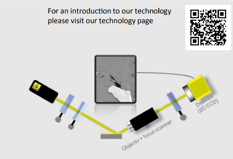
Setup of an imaging ellipsometer including objective and 2D CCD
The ep4 is the latest microscopic imaging spectroscopic ellipsometer with unique measurement capabilities. It can provide real-time ellipsometric enhanced contrast images, and maps of the ellipsometric angles Δ and Ψ . These data can be transferred into Thickness and the complex refractive indices by computerized optical modeling.
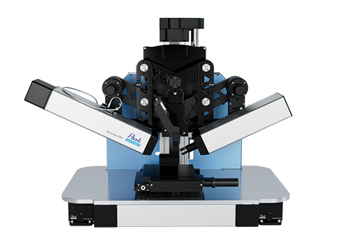
Imaging spectroscopic ellipsometer nanofilm_ep4
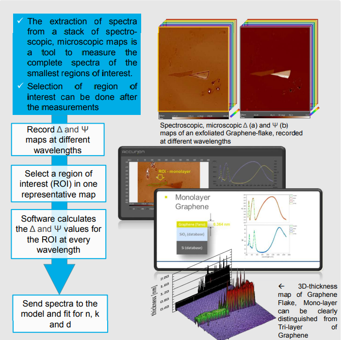
Extracting Spectra of Δ and Ψ
Knife Edge Illumination
| - No contribution by backside reflected light will be recorded. - Non destructive , no treatment of the backside of the sample like roughen, darken, needs to be done. |
Beam cutter in park position (a) and working position (b). |
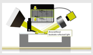
Working principle of a beam cutter
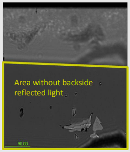
Ellipsometric enhanced contrast micrograph of a MoS2 flake on sapphire.
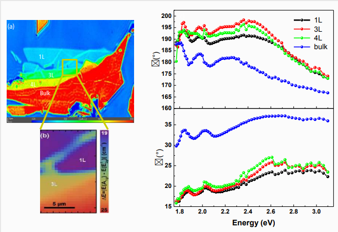
Optical Properties of MoS2
Imaging ellipsometry allows to measure the optical constants from small flakes of e.g. MoS2. Different regions (number of layers) can be measured simultaneously.
(a) Ellipsometric contrast micrograph of MoS2 flake. Cracks and different layers can be seen
(b) Raman mapping to ensure layer-numbers
(c) Measured Δ and Ψ obtained from microscopic mapping
(d) Optical dispersion based on Lorentz- and Tauc-Lorentz oscillators
Pseudo dielectrical function of MoS2 Monolayer
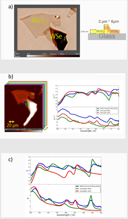
Heterostructure MoS2/WSe2
Investigation of heterostructure of MoS2 monolayer and WSe2 monolayer on glass substrate.
a) shows the ellipsometric enhanced contrast micrograph and the layer structure used for the final modelling. Conventional microscopy can hardly distinguish between monolayers and substrate.
b) shows an exemplary Psi map at 410 nm with the regions used for extracting Delta and Psi spectra (right) in the range of 400 nm – 800 nm.
The resulting dispersions for both monolayer regions and the overlapping hetero-structure are shown in c). The results show no evidence of occurring intralayer excition in the overlapping region
Graphene on Copper
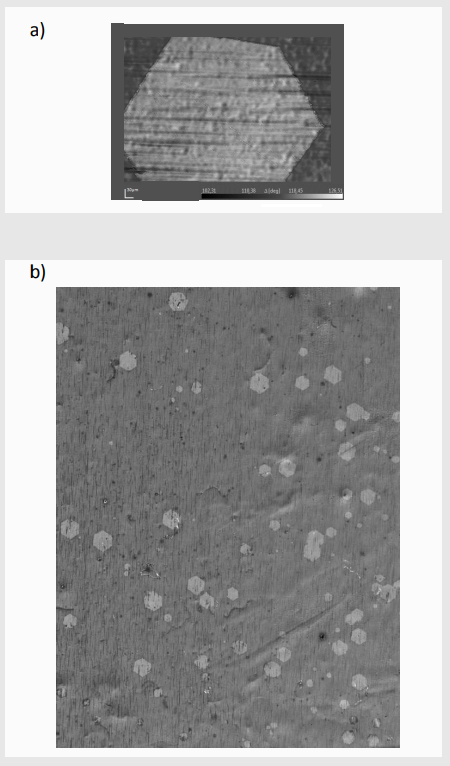
Total coverage of Graphene monolayer islands grown on CuFoil.
a) shows a Delta map of a Graphene monolayer island, that is directly grown on the copper-foil.
Conventional methods don’t work on cu-foil (optical microscopy needs to oxidize the foil) or are not scalable for complete mapping of a foil (SEM; RAMAN).
To handle the waviness of the Cu-foil an auto-focus algorithm is applied and the measurement head of the EP4 is accordingly adjusted in height.
b) shows a complete mapping of a Cu-foil. A surface coverage of 4 % is measured. The hexagonal Graphene islands are also distinguishable from the foil in the wavy part.
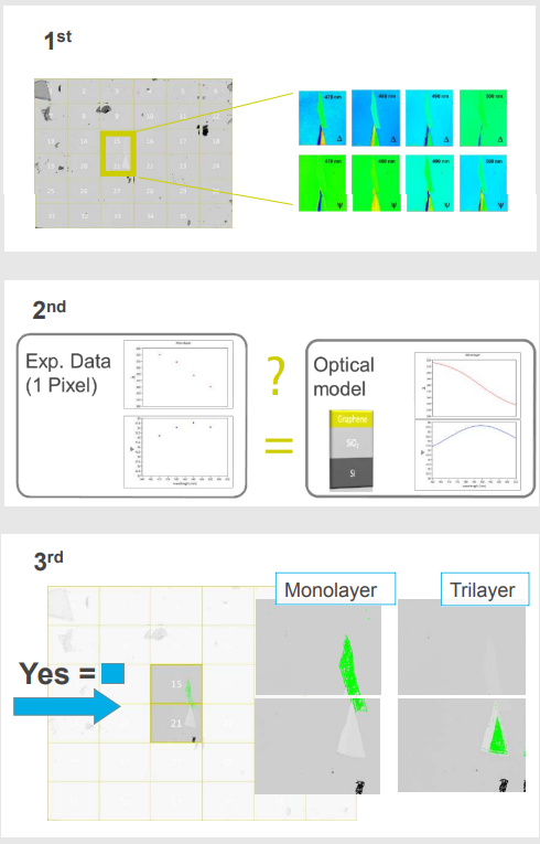
Automatic Flake Search
- Localize areas of desired thicknesses or properties.
- Localizing e.g. flakes by spectroscopic imaging ellipsometry (SIE) depends less on the substrate than conventional methods.
1st Step: Measuring stacks of micro maps at different wavelengths
2nd Step: Comparison optical model - experimental results
3rd Step: Display pixel that are equal to the desired parameter, e.g. Mono- or Trilayer
Method is proven on hBN to look for regions of same thickness and optical properties
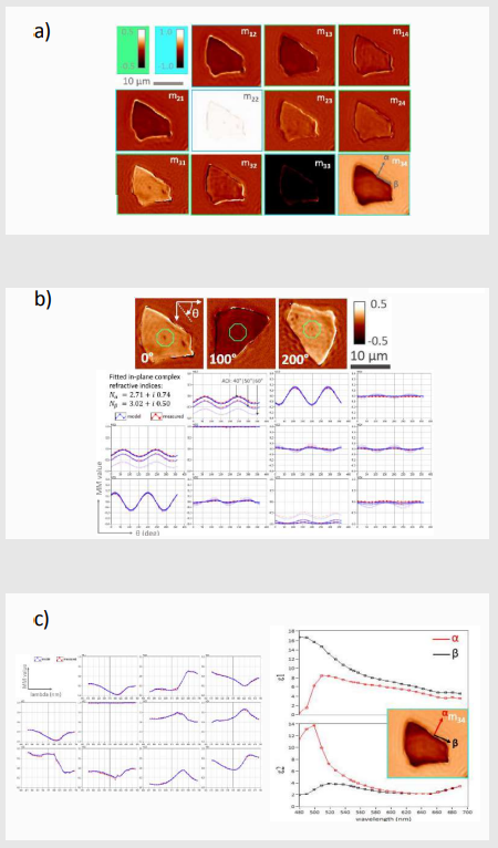
Imaging Müller Matrix of BP
Imaging Mueller-matrix ellipsometry is used to characterize an anisotropic microflake of black Phosphorus.
- a) shows the measured 12 mm-element. The blockoff diagonal elements reveal an anisotropic behaviour for the microflake. Each pixel denotes a measured MM value within a single measurement.
- b) shows exemplary rotational steps of the flake during the theta-spectrum. The resulting spectra for the green region is also shown and reveals an inplane anisotropy.
- c) displays the measured MM lambda spectrum. The fitted dispersion and orientation of the optical axis for the microflake is shown on the right
Hexagonal Boron Nitride
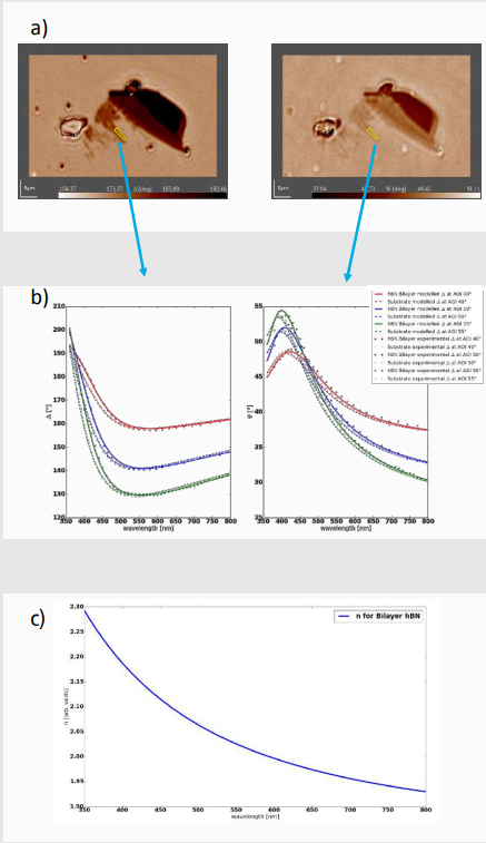
Few layers of hexagonal Boronnitride can be investigated for their spectral dispersion of n.
- a) shows a recorded Δ – map at 430 nm on the left, whereas the image on the right displays measured Ψ–values at 390 nm.
- Spectroscopic maps are recorded in the range of 360 nm to 800 nm.
- b) shows the extracted spectra of Δ and Ψ for the Bilayer hBN and for the substrate at different angle of incidences (AOI).
- Differences between substrate and hBN can be seen around 410 nm.
- The fitted Cauchydispersion for hBN can be seen in c) and is in good agreement with the literature with a refractive around 2.2
