Full Scale Wafer Analysis by Imaging Ellipsometry and Ellipsometric Contrast Micrography (ECM)
S. Funke, P. Braeuninger -Weimer, P. H. Thiesen, S. Hoffmann
Imaging Ellipsometry
Imaging ellipsometry, combines the power of ellipsometry with optical microscopy. It achieves the highest lateral resolution in the field of ellipsometry and offers a very sensitive imaging technology for thin films. Typical samples range from tiny samples like flakes of 2D materials to inhomogeneous surfaces like some CVD grown samples of 2D materials or terraces at epitaxial Graphene surfaces.
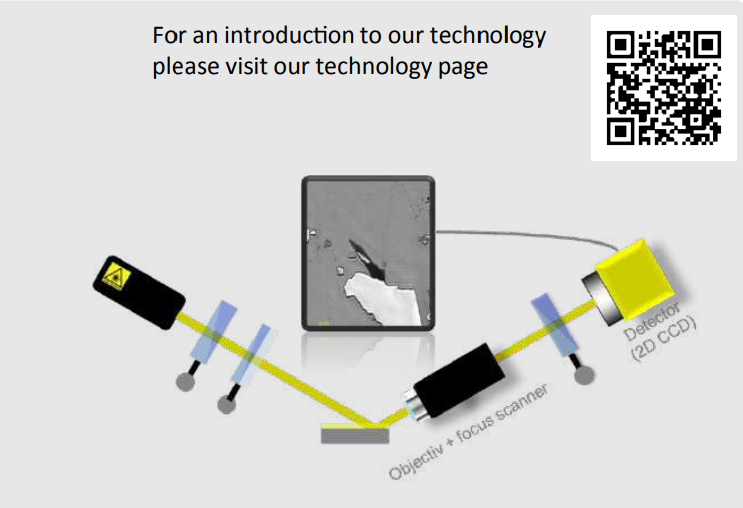
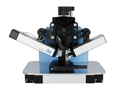
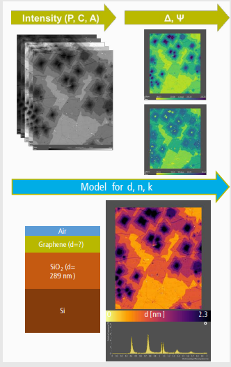
The ep4 is the latest microscopic imaging spectroscopic ellipsometer with unique measurement capabilities. It can provide real-time ellipsometric enhanced contrast images, and maps of the ellipsometric angles Δ and Ψ . These data can be transferred into Thickness and the complex refractive indices by computerized optical modeling.
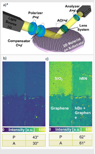
ECM – Contrast Mode
|
The standard setup of an imaging ellipsometer: The lens system and CCD offer a microscopic view on the sample. |
 |
Ellipsometry Mode
|
For the ellipsometry mode contrast images are taken for different rotational angles of |
 |
Optical Properties of MoS2/WSe2
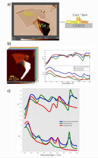
a): The ellipsometric enhanced contrast micrograph and the layer structure used for the final modelling.
Conventional microscopy can hardly distinguish between monolayers and substrates.
b): An exemplary Psi map at 410 nm with the regions used for extracting Delta and Psi spectra (right) in the range of 400 nm – 800 nm.
The resulting dispersions for all regions are shown in
c). The measurement and analysis is done simultaneously for all regions
ECM Compared to Other Methods
|
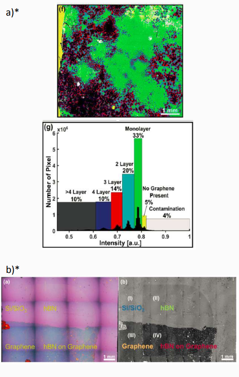
a): The same region of Graphene on 300 nm SiO2 measured by Raman-mapping, Optical Microscopy (OM), b): The histogram of each method shows best distinguishing for the ellipsometry mode. |
 |
Graphene on Copper
|
a): ECM stitching obtains a large sample overview. False coloring according to layer number as depicted |
 |
Graphene on Cu-foil as Grown
a): ECM stitching obtains a large sample overview. False coloring according to layer number as depicted in the histogram. For the overview ECM images are recorded with an motorized XY-stage and stitched seamlessly. The histogram can be used to calculate layer coverage ratios. In figure b) another comparison of OM and ECM is shown. The different regions of stacked 2D materials can be hardly distinguished in the OM (left) image, but very well in the ECM Image on the right.
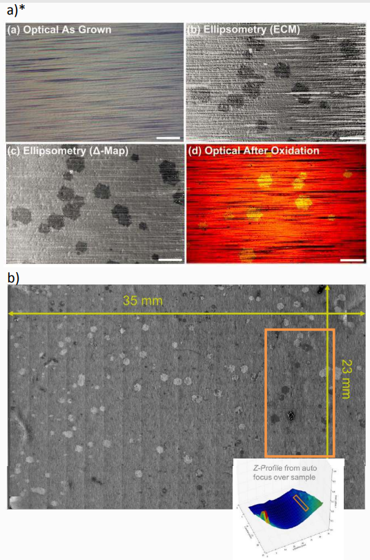
Further investigations at the flipped contrasts are done. Figure c) shows a Graphene hexagon with two different regions (flipped and non-flipped contrast). Spectroscopic imaging ellipsometry measurements are done for the Regions of interest (ROI) shown in grey shapes in the Ψ map. The resulting spectra are shown in d). The optical modeling yields the refractive indices for the Copper, Graphene and the Copper-oxide (figure e)). The contrast flip is not induced by the curvature of the foil, but by the partial oxidation of the Copper.
Full 4“ Wafer Scan
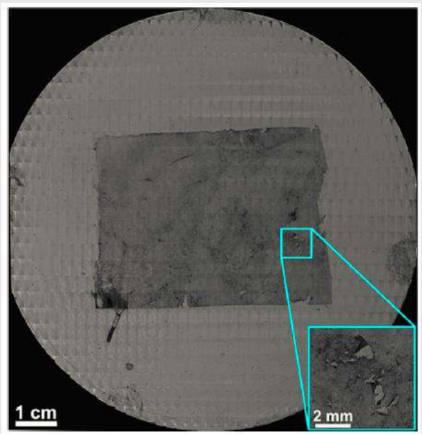
The figure above shows a 4” native – Silicon wafer, that is partially covered with Graphene monolayer. Conventional method for fast analysis are not able to distinguish Graphene monolayer on native Silicon, but ECM is. The complete scan is done within 47 minutes and reveals defects, contaminations and cracks as small as 10 µm.
