Spectroscopic Ellipsometry and Optical Constants of MoS2 Flakes
E. Parzinger, S. Funke, B. Miller, P. Thiesen, A. W. Holleitner, and U. Wurstbauer
Introduction
Transition Metal Dichalcogenides, e.g. MoS2 mono- and fewlayers are atomistic thin semiconductors with a band gap in the visible range featuring extremely high light absorption efficiency as well as strong excitonic properties making the material of great interest for both fundamental research as well as for optoelectronic applications. Since the optical properties of MoS2 strongly dependent on the number of layers, a layer selective knowledge of the optical constants is demanding. Refractive index (n) and extinction parameter (k) are fundamental to describe the light-matter interaction of the material.
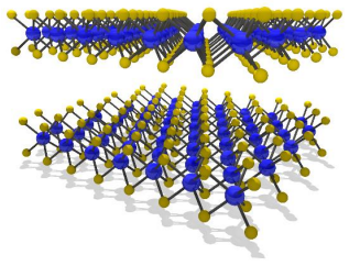
We report on the imaging intensity and spectroscopic ellipsometry (SE) on mechanically exfoliated MoS2 flakes transferred to Si/SiO2 and sapphire substrates. The outstanding lateral resolution of ~1µm [1] enables the layer selective extraction of the optical constants from SE and the study of their lateral uniformity. Contrary to reflectance spectra [2], SE is sensitive not only to the in-plane but also to the out-of-plane component of the optical constants. We have extracted both components of the optical constants using an anisotropic model. Number of layers, as well as intrinsic doping density and lateral homogeneity have been studied by complementary µ-Raman spectroscopy.
Imaging ellipsometry set-up
(Imaging) Ellipsometry:
non-destructive method to determine optical properties with high lateral resolution. Change in the polarization of the reflected light is measured.
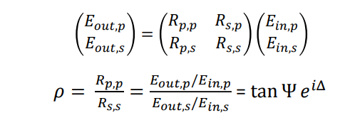
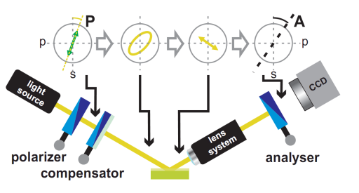
PCSA configuration
=> beam linear polarized after reflection
=> Intensity-minimum measured by 90° positioned analyzer (‘nulling condition’)
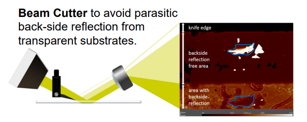
The Knife edge at the top, the flake in the backside-reflection free area and the shadow of the flake in the backside reflection area.
Imaging ellipsometry (IE) – exfoliated MoS2 on SiO2
Optical microscopy image, imaging ellipsometry contrast map and monochromatic reflectivity map of aMoS2 flake on Si/SiO2. Mono, bi, triand multilayer regions can be distinguished from all methods with a high lateral resolution of less than 1 µm.
Contrast in the region of band gap weak for MoS2 on SiO2 => Spectroscopic ellipsometry and modeling of ellipsometric angles to determine optical constants is difficult and requires different substrate (e.g. sapphire)
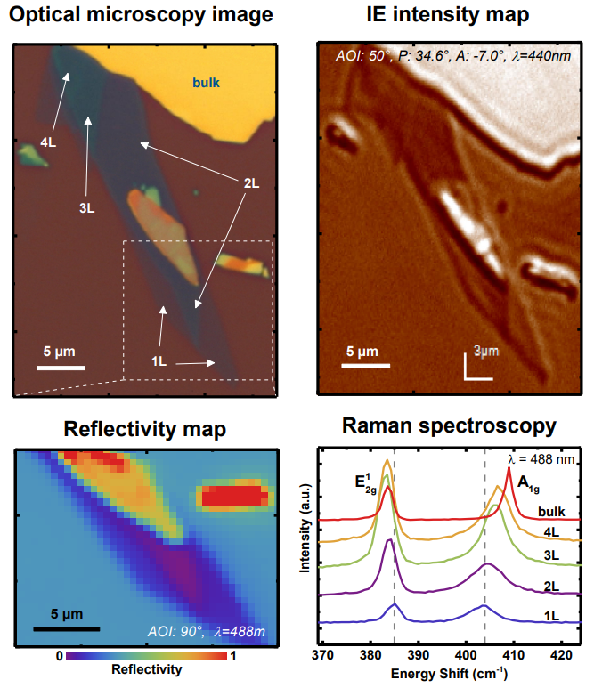
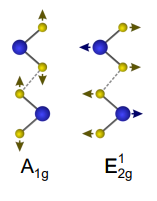
Raman spectroscopy of A1g and E1 2g mode is used to determine the number of layers.
Spectroscopic ellipsometry – exfoliated MoS2 on sapphire
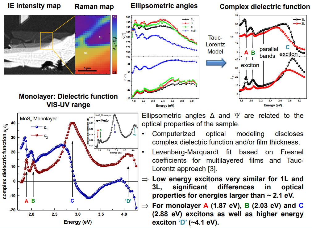
Lateral variation of dielectric function
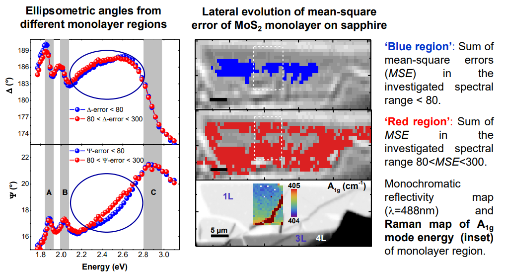
• Lateral variation of MSE mainly dictated by spectra range between B and C excitons (2.2 eV – 2.7 eV).
• Energy of A1g phonon mode sensitive probe for changes in charge carrier density [4]: Mode energy continuously decreases towards sample edge by about ΔE 0.5cm-1 corresponding to change in charge carrier density Δn> 21012 cm-2.
• No spatial correlation between change in Raman modes and variations in MSE ⇒ MSE not dependent on change in charge carrier density.
• Variation in MSE might be caused by altered van der Waals interact between MoS2 & substrate.
Anisotropic dielectric function
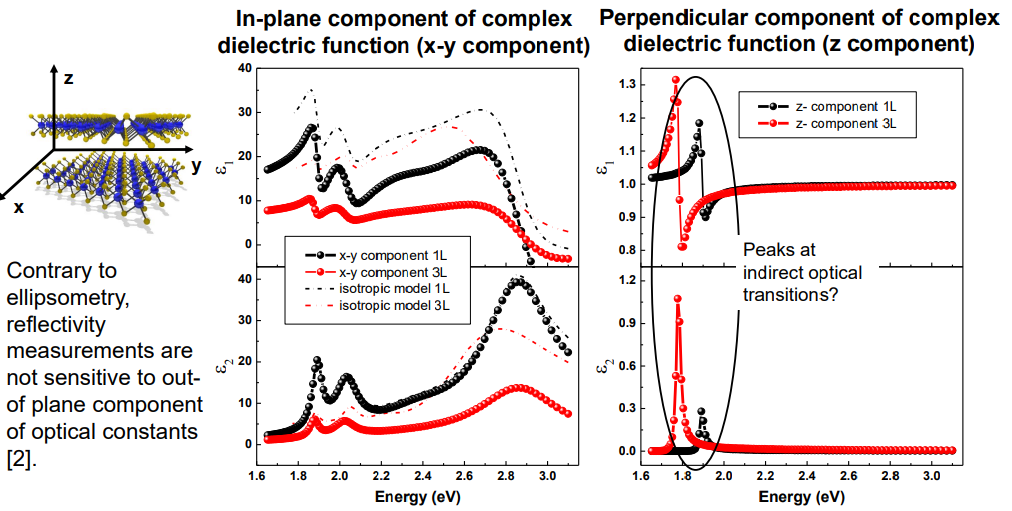
• Levenberg-Marquardt fit based on Fresnel coefficients for multilayered films and Tauc-Lorentz approach [3] assuming anisotropic dielectric functions in-plane (x-y plane) and out-of-plane (z direction).
• Dielectric function in visible range dominated by x-y component, however finite contribution in zdirection around the band gap for 1L as well as for 3L.
• For 1L: peak of ε2 in z-direction at slightly larger energy compared to x-y component.
• For 3L :peak of ε2 in z-direction at slightly lower energy compared to x-y component.
=> Transitions in z-direction are assigned to indirect transitions close to Γ-point of the band structure opposite to the direct A, B and C excitonic transitions observable in x-y plane.
References
[1] U. Wurstbauer, et al. Appl. Phys. Lett. 97, 231901 (2010).
[2] Y. Li, A. et al. Phys. Rev. B 90, 205422 (2014).
[3] EP4 Model from Accurion GmbH, Göttingen.
[4] B. Miller, et al. Appl. Phys. Lett. 106, 122103 (2015).
[5] S. Funke et al. (2015).
[6] E. Parzinger et al. (2015)
Acknowledgements
We acknowledge support by the DFG excellence cluster “Nanosystems Initiative Munich” (NIM), the Center for NanoScience (CeNS) in Munich and BaCaTec.
