 “In terms of the scope and throughput of the automation, the 300mm bare wafer ADR is the one and only AFM solution from Park without any match in the market,” stated Ryan (YK) Yoo, Vice President of Global Sales and Marketing.
Santa Clara, CA April 01, 2014
Park Systems, a leading manufacturer of atomic force microscopy (AFM) products, proudly introduces the Automatic Defect Review (ADR)AFM for 300mm bare wafers, a fully automated AFM solution that improves throughput of AFM defect review by up to 1,000%. The 300mm bare wafer ADR AFM is a new process for identifying defects designed specifically for the semiconductor market without the need of reference markers. In terms of accuracy and productivity, Park’s new ADR process speeds up and improves the way defects are imaged and analyzed compared with more traditional manual AFM methods of defect review on the market. Furthermore, it is able to do this without the laborious and often damaging reference marks created on a sample wafer. Additionally, this new Park ADR AFM offers a significantly longer tip life than those of competitors by 10x~20x thanks to Park’s ground breaking True Non-Contact™ Mode AFM technology.
“This new advanced Park ADR solution is designed specifically for semiconductor engineers and researchers to replace the old process of identifying nanoscale defects by manual AFM which was time consuming and greatly hindering the throughput,” comments Sang-il Park, Chairman and CEO Park Systems. “We used our highly successful automated AFM solution widely accepted as the industry standard in the hard disk market to develop a new ADR capability for the semiconductor industry with the clear goal of improving accuracy and productivity for our customers.”
The new 300mm bare wafer ADR provides a fully automated defect review process by AFM from transfer and alignment of defect maps to the survey and zoom-in scan imaging of defects that uses a unique remapping process that does not require any reference marker on a sample wafer. Unlike SEM which leaves destructive irradiation marks, square-shaped, on defect sites after its run, the new Park ADR AFM enables advanced coordinate translation with enhanced vision that uses the wafer edge and notch to automatically enable the linkage between a defect inspection tool and Park AFM. Since it is fully automated, it does not require any separate step to calibrate the stage of the targeted defect inspection system, increasing throughput by up to 1,000 percent.
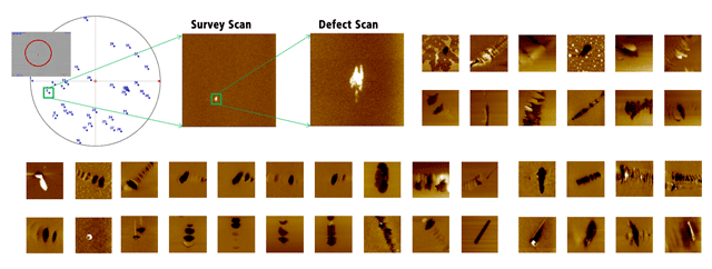
By utilizing Park’s proprietary coordinate translation technique, the new Park ADR AFM can accurately transfer the defect maps obtained from a laser-scattering defect inspection tool to a 300mm Park AFM system. This allows the AFM for high throughput, fully automated defect imaging. The defects are imaged in two steps; (1) a larger, survey scan image to refine the location, then (2) a smaller, zoom-in scan image to obtain the details of the defect, presenting automatic analysis of the defect type and the subsequent defect dimensions.
Previously, defect review using Scanning Electron Microscope (SEM) has been used to image the defects of a bare wafer after defect sites are mapped by the laser-scattering defect inspection tools such as Surfscan from KLA-Tencor. However, the imaging by defect review SEM is limited to 2D and cannot provide the 3D information that is now available with Park’s new ADR AFM and is critical for bare wafer manufacturing control.
“In terms of the scope and throughput of the automation, the 300mm bare wafer ADR is the one and only AFM solution from Park without any match in the market,” stated Ryan (YK) Yoo, Vice President of Global Sales and Marketing. “We designed this product solution specifically to create higher profit margins for semiconductor customers by increasing throughput in the defect review process in a highly competitive manufacturing environment.”
The success rate of the 300mm bare wafer ADR by AFM depends on two factors: the accuracy of stage mapping and the size of the initial survey scan. With more accurate stage mapping, a smaller survey scan size can be used that greatly increases the chance of correctly identifying defects. The new 300mm bare wafer ADR process by Park AFM vastly improves the stage mapping accuracy by adopting an advanced remapping algorithm and enhanced vision technique. In the new 300mm bare wafer ADR process, the RMS position error of survey scans are less than 5 µm. It means that all the defects are located within 5 µm using the defect map provided from a defect inspection tool. Combined with the much smaller position error of defect location, the success rate typically reaches higher than 95%.
Currently, there is no other solution that can match the scope and throughput of the new ADR automation process only available at Park Systems for 300mm bare wafer analysis. It is the only solution with fully automated defect review process, from transfer and alignment of defect maps to the survey and zoom-in scan, imaging of defects without any need of reference markers.
About Park Systems
Park Systems is a world-leading manufacturer of atomic force microscopy (AFM) systems with a complete range of products for researchers and industry engineers in chemistry, materials, physics, life sciences, semiconductor and data storage industries. Park’s products are used by over a thousand of institutions and corporations worldwide. Park’s AFM provides highest data accuracy at nanoscale resolution, superior productivity, and lowest operating cost thanks to its unique technology and innovative engineering. Park Systems, Inc. is headquartered in Santa Clara, California with its global manufacturing, and R&D headquarters in Korea. Park’s products are sold and supported worldwide with regional headquarters in the US, Korea, Japan, and Singapore, and distribution partners throughout Europe, Asia, and America. Please visit http://www.parkafm.com or call 408-986-1110 for more information.
