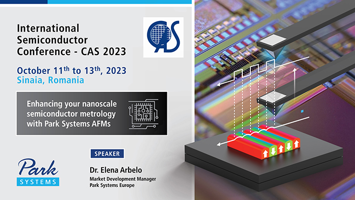
Park Systems and Schaefer SouthEast Europe srl will be exhibiting together at the 46th edition of the annual International Semiconductor Conference – CAS 2023. The Conference will take place on October 11-13 in Sinaia, Romania, at Hotel Sinaia and is not only targeting semiconductor electronics, but also micro-and nanotechnologies (including micro-nanosystems).
- Date: October 11th – 13th 2023
- Location: Hotel Sinaia , Bulevardul Carol I 8, Sinaia 106100, Romania
- Topics: semiconductor device physics, technology and integrated circuits to micro- and nanotechnologies, including micro-nanoelectronics and micro-nanosystems technologies, encompassing all relevant aspects such as modelling and simulation, design, measurement.
Visit our shared booth and join our talk to learn more about our cutting-edge AFM solutions that enable you to become more efficient, more accurate and more productive in your research.
______________________________________________________________________________________________________________

Join Dr. Elena Arbelo, Market Development Manager, Park Systems Europe at the CAS 2023 for her talk
- ⏩ TALK: “Enhancing your nanoscale semiconductor metrology with Park Systems AFMs”
- ⏩ DATE: Thursday October 12, 2023 between 09:00 an 11:00 am
ABSTRACT
Author: Dr. James Kerfoot¹
¹Park Systems UK Ltd, MediCity Nottingham, D6 Thane Rd, Nottingham, UK, NG90 6BH
Among all state-of-the-art characterisation techniques, atomic force microscopy (AFM) is a particularly powerful tool in the study of semiconductors since it enables device morphology and a host of functional properties to be mapped with nanometre scale resolution or better. In this presentation, the application of AFM and its functional modes to semiconducting materials will be explored for a range of examples. Additionally, we will emphasise how automation and ease-of-use features integrated into AFMs from Park Systems enables such data to be acquired less laboriously and more reproducibly.

In our first test case, we explore how AFM can be used to measure the morphology of semiconductor devices. We will give examples showing how automated data acquisition and robotics improves throughput and reproducibility of both feature sizes and roughness measurements before moving on to measurements of sidewalls of etched structures which exhibit an undercut.
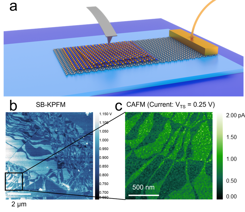
We will then move on to examine the underlying principles of both Kelvin probe force microscopy and conductive AFM. This will be applied to the study layered materials where controlling the twist angle between flakes leads to interfacial ferroelectricity [1-3]. We then discuss different ways in which such domains may be mapped and manipulated both electrically and mechanically [3,5]. We utilise CAFM (where a tunnelling current is measured across a bilayer of parallel stacked hBN) to systematically study the variation of domain morphology versus mechanical setpoint and tip-sample bias in a configuration analogous to a tunnelling transistor.
In the final section, we will give examples of the use of AFM as a failure analysis tool via both scanning capacitance microscopy (SCM) to spatially map dopant concentration and type in semiconductor devices and dielectric breakdown measurements with high voltage AFM. Throughout the talk, we will show how Park Systems AFMs meet the needs of modern semiconductor research with both enhanced automation and a toolbox of functional modes to explore electronic properties on the nanoscale.
Fig. 1. Parallel stacked hBN may be formed by breaking and restacking exfoliated layers mechanically (a). Once formed, these structures may be characterised using KPFM to map the morphology of ferroelectric domains (b). For sufficiently thin layers (~0.6 nm), tunnelling current may be mapped using CAFM.
References:
[1] C. R. Woods et al. Nat Commun. 12, 347 (2021).
[2] K. Yasuda et al. Science 372, 6549 1458 (2021)
[3] M. Vizner Stern et al. Science 372, 6549, 1462, (2021).
[4] Q. Zhao et al. J. Phys. Mater. 3 016001 (2020)
[5] O. Kolosov et al. Phys. Rev. Lett. 74, 4309 (1995)
_____________________________________________________________________________________________________________
About CAS:
Organized in Romania yearly since 1978 as Annual Semiconductor Conference (acronym CAS). Starting in 1991, CAS was opened to the international scientific community and changed its name accordingly to the International Semiconductor Conference, still maintaining the same acronym (CAS) and has been an IEEE event since 1995. In the last two decades, the conference was frequently accompanied by satellite events, such workshops organized by FP6 and FP7 European Projects.
