-
LiBattery Workfunction UTEM hetero_structure Piranha mechanical_property Growing Oxidation Composition Magnetic LateralPFM PinpointPFM AM-KPFM organic_polymer cannabidiol sputter Adhesive Ceramics Polyvinylidene_fluoride TungstenDeposition YszSubstrate StrontiumTitanate ThermalDetectors Forevision BismuthVanadate Lateral Pore TipBiasMode Vacuum PvdfBead electrospinning CancerCell TemperatureControllerAFM ScratchMode molecule
Report image
If you found this image unacceptable, please let us know. We will review your report and take action if we determine this image is really unacceptable.
ITO Film Sputter Deposited onto Silicon
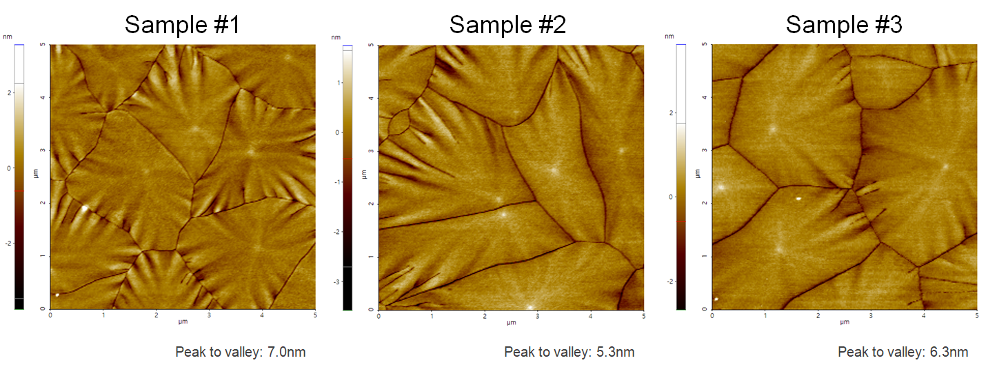
ITO-film, which was sputter deposited onto silicon. The grain size of those samples was influenced by changing the process settings in the Cluterline RAD sputter deposition system, one of the deposition tool platforms manufactured by Evatec.
Scanning Conditions
- System: NX10
- Scan Mode: Non-contact
- Cantilever: PPP-EFM (k=2.8N/m, f=75kHz)
- Scan Size: 5μm×5μm
- Scan Rate: 0.1Hz
- Pixel Size: 256 × 256
- Scan Mode: Non-contact
- Cantilever: PPP-EFM (k=2.8N/m, f=75kHz)
- Scan Size: 5μm×5μm
- Scan Rate: 0.1Hz
- Pixel Size: 256 × 256