-
Au111 alkanes dielectric trench TungstenDeposition IIT-chennai Austenite PvdfFilm Korea FM-KPFM UnivMaryland Boron GalliumPhosphide Polypropylene Wafer HafniumDioxide HydroGel fluoroaalkane Celebration Silver Butterfly Ni-FeAlloy ContactMode Magnetic Force Microscopy vertical_PFM polymeric_arrays MechanicalProperty LightEmiting InLiquid C_AFM atomic_layer ScanningThermalMicroscopy doped Cell Optoelectonics MetalCompound
Report image
If you found this image unacceptable, please let us know. We will review your report and take action if we determine this image is really unacceptable.
WLI image of wafer ID mark
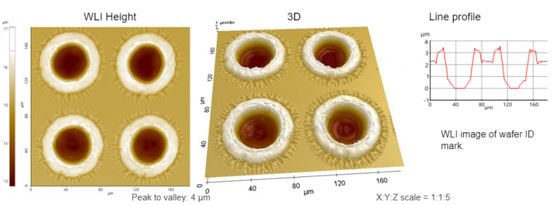
Scanning Conditions
- System : NX-Hybrid WLI
- Scan Mode: WLI
- Field of view: 182μm×182μm