-
Bismuth Optical FastScan Hexatriacontane Aluminum LiNbO3 PolyvinylAcetate ConductiveAFM Galfenol mechanical property HACrystal GaN GlassTemp Tin disulfide Inorganic temp Conducting TriGlycineSulphate Sperm Vinylpyridine ScanningKelvinProbeMicroscopy semifluorinated alkane strontiu_titanate Typhimurium SICM nanomechanical MembraneFilter STO Nanostructure UnivCollegeLondon Stiffness PolymerPatterns EvatecAG TransitionMetal 2dMaterials
Report image
If you found this image unacceptable, please let us know. We will review your report and take action if we determine this image is really unacceptable.
Christmas Ball Lithography on Si
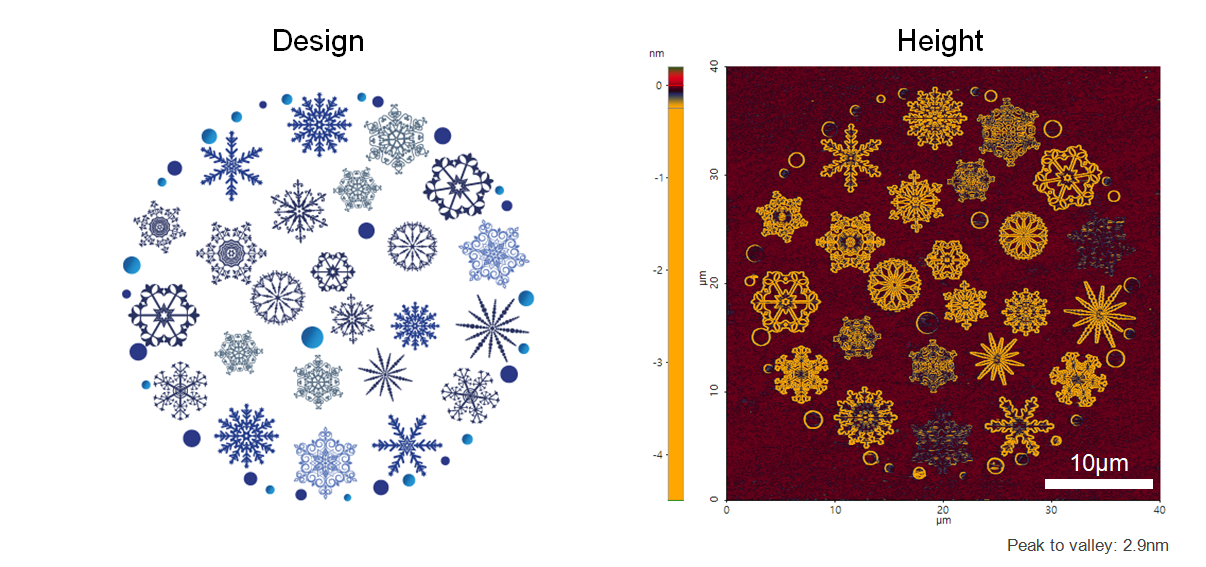
Create oxidation layers on bare Si surface using bias mode of lithography.
Scanning Conditions
- System: NX10
- Scan Mode: Lithography
- Cantilever: AD-40-SS (k=40N/m, f=200kHz)
- Scan Size: 40μm×40μm
- Scan Rate: 0.5Hz
- Pixel Size: 1024 × 1024
- Tip Bias: -10V for patterened area
- Scan Mode: Lithography
- Cantilever: AD-40-SS (k=40N/m, f=200kHz)
- Scan Size: 40μm×40μm
- Scan Rate: 0.5Hz
- Pixel Size: 1024 × 1024
- Tip Bias: -10V for patterened area