-
heterojunctions TungstenDeposition ReflexLens flakes Butterfly HighResolution SurfaceOxidation TiO2 Dopped Adhesive Temperature MolybdenumDisulfide ScanningThermalMicroscopy SICM CrossSection LDPE Solar Thermoplastic_polyurethane Tungsten FuelCell semifluorinated alkane OpticalWaveguides HafniumDioxide Anneal Metal Protein molecules Magnets OxideLayer InorganicCompound NUS_NNI_Nanocore BiasMode Materials lift_mode Temasek_Lab
Report image
If you found this image unacceptable, please let us know. We will review your report and take action if we determine this image is really unacceptable.
Moire pattern of MoS₂-WSe₂
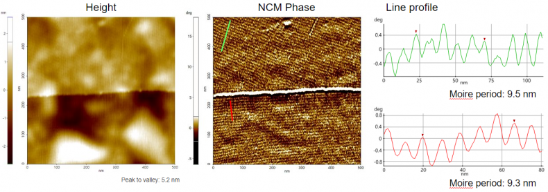
Scanning Conditions
- System : FX40
- Scan Mode: Tapping
- Scan Rate : 3Hz
- Scan Size : 500nm×500nm
- Pixel Size : 512×512
- Cantilever : PPP-FMR (k=2.8N/m, f=75kHz)