-
AM_SKPM MoirePattern Materials PiezoelectricForceMicroscopy align Croatia Solution #EC Transparent DentalProsthesis OxideLayer LMF molecule organic_polymer Sapphire PolyvinylAcetate STM Treatment Cell Piezoelectric Optical Ferroelectric FrictionForce Titanate OpticalWaveguides LiquidCrystal dielectric_trench Sulfur Aluminium_Oxide Oxidation ElectroChemical biocompatible LiftHeight PolyvinylideneFluoride Ptfe
Report image
If you found this image unacceptable, please let us know. We will review your report and take action if we determine this image is really unacceptable.
hBN-few layer Graphene
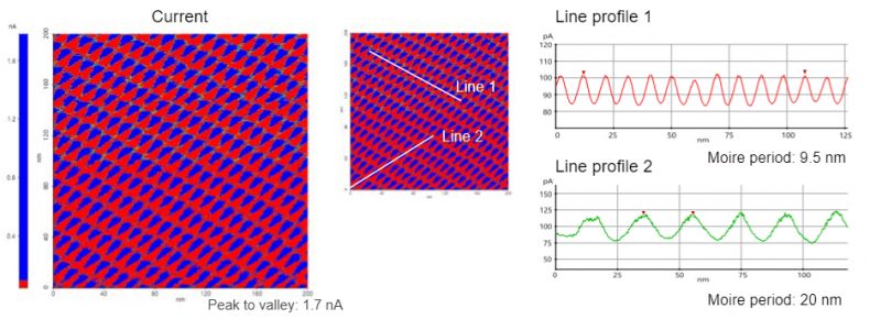
Scanning Conditions
- System : NX10
- Sample bias: 1.75 V
- Scan Mode: C-AFM
- Scan Rate : ALL 0.5Hz
- Scan Size : 200nm×200nm
- Pixel Size : 2048×2048
- Cantilever : AD-2.8-AS (k=2.8N/m, f=75kHz)