Wednesday, 29 April 2020
- 10:00 am – 11:30 am
(GMT)
London, Dublin - 11:00 am – 12:30 pm
(CEST)
Berlin, Paris, Rome - 18:00pm – 19:30 pm
[UTC+9]
Seoul, Tokyo -

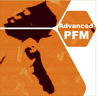
The application the ferroelectric materials in communication and information technology or data storage continuously increases. The optimization ferroelectric devices and investigation of novel applications, such as energy harvesting, are of great interest for the scientific community and require characterization techniques that can access nanoscopic domain patterns. Here, piezoresponse force microscopy (PFM), a contact mode Atomic Force Microscopy method, provides real-space domain information with a nanometer resolution.
In this webinar, we provide an overview and introduction of three available PFM modes: Off-resonance single frequency PFM, resonance-enhanced single frequency PFM and dual frequency resonance tracking (DFRT) PFM. Each of the modes comes with advantages and disadvantages depending on the piezoelectric and topographic properties of the investigated samples. To help you exploit the full potential of PFM, we will to provide you with the information which mode is most suitable for your samples.

Presented By :
Ilka Hermes - Principle Scientist Park Systems Europe, Mannheim, Germany
ihermes@parksystems.com
Ilka is the principle scientist at Park Systems Europe, where she maintains and supports scientific collaborations to establish new research projects.
Prior, she worked at the Max Planck Institute for Polymer Research (Main Germany) in the group of Stefan Weber to investigate perovskite solar cells with electrical Atomic Force Microscopy (AFM) modes, and at the Johannes Gutenberg University Mainz in the group of Angelika Kühnle to characterize liquid-solid interfaces with high resolution AFM. Ilka’s primary fields of expertise include Piezoresponse Force Microscopy (PFM), Kelvin Probe Force Microscopy (KFM), and conductive AFM on semiconducting and/or ferroelectric devices.


