SANTA CLARA, Calif., June 6, 2019
Park Systems, a leader in Atomic Force Microscopy (AFM) since 1997 is hosting their annual free AFM Luncheon for all SEMICON West attendees and Park customers on July 10, 2019 from 12-2pm at ThirstyBearBrewing Company located at 661 Howard Street, San Francisco, less than a 5-minute walk from South Hall of the Moscone Center. The featured speaker at this year's luncheon is Dr. Bongsub Lee, a senior manager of metrology and characterization at Xperi Corporation, who will present on the topic, Characterizing Nanoscale Topography for Direct Bond Interconnect. Registration for the luncheon is ongoing and can be done online at parksystems.com/semiconwest2019.

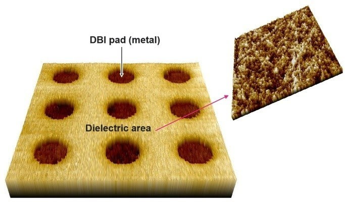
Examples of 3-dimensionally represented AFM data from a DBI® sample.
It consists of SiO2 background and recessed Cu pads.
Also shown is a magnified view of the SiO2 surface, which should have
a sufficiently low roughness for direct bonding.
"Characterizing and controlling nanoscale topography is essential for achieving DBI®," comments Dr. Bongsub Lee, whose current interest is 3D-IC technology based on direct bonding of device wafers and die. "Atomic Force Microscopy (AFM) is a critical technique required to monitor the CMP process module and ensure a robust manufacturing process."
Direct Bond Interconnect (DBI®) achieves mechanical and electrical connection between device wafers or die by directly joining the dielectric and metal surfaces. It enables very fine pitch interconnects for high bandwidth 3-dimensional integrated circuits (3D-IC). DBI® is currently used for mass production of image sensors for mobile phones and is actively investigated for DRAM, NAND, and MEMS applications.
Recently Park Systems received major orders for its automated Atomic Force Microscopy (AFM) for wafer production metrology from 18 of the top 20 semiconductor manufacturers. To learn more about Park Systems, visit their booth 1531 at SEMICON West where they will be exhibiting their full line of AFM equipment.
Park Systems cost saving value proposition innovations for semiconductor manufacturers include Park NX-Wafer, designed specifically for the semiconductor industry and improving productivity by up to 1000%. Park NX-Wafer is the only wafer fab Atomic Force Microscope with automatic defect review and True Non-Contact™ Mode AFM enabling a critical inline process to classify defect types and source their origin through high resolution 3D imaging, scanning capacitance microscopy and scanning spreading resistance microscopy.
Park Systems is hosting NanoScientific Symposiums world-wide including the 2nd annual NanoScientific Symposium at their Park NanoScience Center at SUNY Polytechnic Institute. Abstracts for speaker opportunities are being accepted until August, please submit here http://parksystems.com/spm2019.
About Park Systems
Park Systems is a world-leading manufacturer of atomic force microscopy (AFM) systems with a complete range of products for researchers and industry engineers in the chemistry, materials, physics, life sciences, and semiconductor and data storage industries. Park’s products are used by more than a thousand institutions and corporations worldwide. Park’s AFM provides the highest data accuracy at nanoscale resolution, superior productivity, and the lowest operating cost, thanks to its unique technology and innovative engineering. Park Systems, Inc. is headquartered in Santa Clara, California with its global manufacturing and R&D headquarters in Korea. Park’s products are sold and supported worldwide with regional headquarters in the US, Korea, Japan, Singapore, Germany, China and Mexico, and distribution partners throughout Europe, Asia, and the Americas. Please visit http://www.parksystems.com or call 408-986-1110 for more information.
