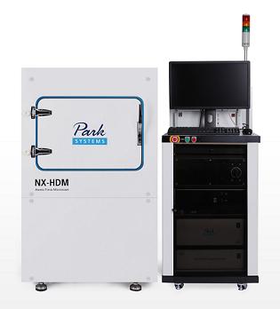
Park Systems, world leader in atomic force microscopy (AFM) for the semiconductor and hard disk markets introduces Park NX-HDM, a fully automated automatic defect review and sub-angstrom surface roughness atomic force microscopy (AFM) system for device substrates and disk media, the first metrology tool capable of providing this level of accuracy and automation. The NX-HDM system sets a new standard for the industry in automatic defect review AFM technology by increasing throughput up to 1000 percent and an offering of 30% higher success rate than prior system, analyzing, identifying and scanning media for all wafer sizes up to 150mm.

Park NX-HDM
Park Systems, world leader in atomic force microscopy (AFM) for the semiconductor and hard disk markets introduces Park NX-HDM, a fully automated automatic defect review and sub-angstrom surface roughness atomic force microscopy (AFM) system for device substrates and disk media, the first metrology tool capable of providing this level of accuracy and automation. The NX-HDM system sets a new standard for the industry in automatic defect review AFM technology by increasing throughput up to 1000 percent and an offering of 30% higher success rate than prior system, analyzing, identifying and scanning media for all wafer sizes up to 150mm.
“For researchers working with hard disk media and other flat substrates, the process of identifying nanoscale defects is time consuming with conventional tools, hindering throughput. The Automatic Defect Review (ADR) speeds up and improves the way it identifies, scans and analyzes defects in substrates and media,” comments Sang-il Park, CEO and Chairman. “Beta test runs with Park NX-HDM demonstrate a 10x increase in throughput for defect review in an automated process when compared with more traditional manual methods of defect review. Moreover, we perfected the remapping and defect identification algorithm, and the success rate of the new NX-HDM is 30% higher than its previous generation, XE-HDM.”
Park NX-HDM for HDD, LED, solar, and general semiconductor device industries, speeds up the automatic defect review for media and substrates. The survey scan, zoom-in scan, and analysis of imaged defect types are automated with wide range of automated optical inspection (AOI) tools. In addition, True Non-Contact Mode™, combined with the industry’s lowest noise floor, provides accurate and reliable measurements for the sub-angstrom surface roughness of diverse media and substrates.
The unique Park dual servo system with two symmetric, low-noise position sensors are incorporated on each axis of the XY scanner to retain a high scan orthogonality for widescan ranges and sample sizes. The secondary sensor corrects and compensates for non-linear and non-planar positional errors caused by a single sensor.
“There has never been a metrology tool capable of providing accurate and reliable measurements for the sub-Angstrom roughness of the substrate surfaces,” said Ryan Yoo, Vice President of Global Sales and Marketing. “By delivering the industry’s lowest noise floor of less than 0.5Å, Park NX-HDM can acquire accurate, repeatable, and reproducible sub-angstrom roughness measurements for the flattest substrates and media.”
Suppliers to various industries are developing ultra-flat substrates to address the ever-increasing need for shrinking device dimensions. However, there has never been a metrology tool capable of providing accurate and reliable measurements for the sub-Angstrom roughness of this substrate surfaces. Park NX-HDM combines the industry’s lowest noise floor of less than 0.5 angstrom with Park’s proprietary True Non-ContactTM technology to create repeatable and reproducible sub-Angstrom roughness measurements without tip degradation. Parameters of scan size and scan speed are adjustable to match user’s needs in throughput and quality control.
With the release of Park NX-HDM, Park Systems retains its leadership in automated industrial atomic force microscopy while pushing the envelope of the AFM technology to meet the ever sophisticated demands from the semiconductor and disk storage industries. Technical data and sample measurements are available on request. For more information please contact psi@parkAFM.com or visit http://www.parkAFM.com.
