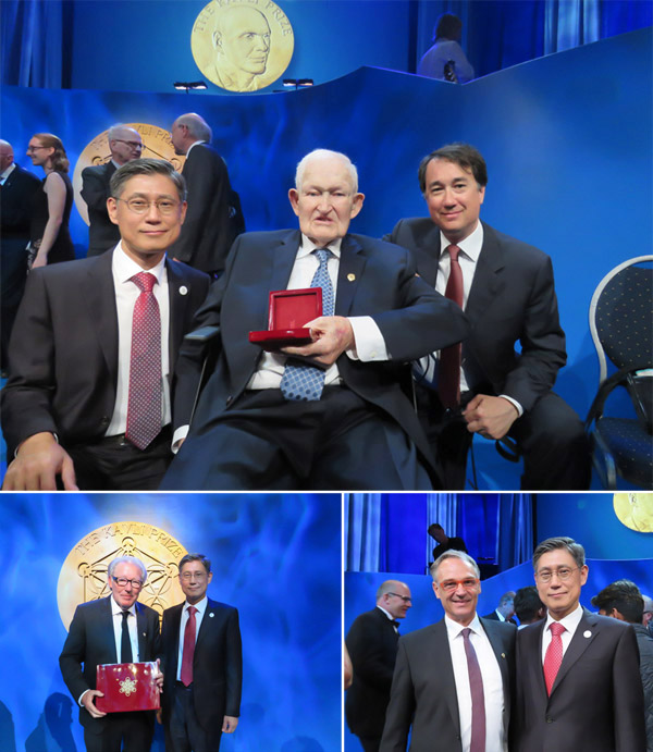
Dr. Sang-il Park, the founder and CEO of Park Systems was one of the researchers at Stanford University when the first AFM technology was developed by Dr. Calvin Quate, Gerd Binnig and Christoph Gerber and other researchers. Dr. Park, recognizing the potential of AFM technology for a wide range of fields was the first to commercialize AFM and since then thru innovation and collaboration with customers, Park has become a global leader in AFM manufacturing.
How AFM was born - recounted by Dr. Calvin Quate during his Kavli Prize award speech (excerpt)
The STM was a big scientific achievement. In fact, the inventors, Gerd Binnig and Heinrich Rohrer, went on to earn a Nobel Prize in physics in 1986 for their work on the STM. However, the STM had a major limitation. Since it depended on the flow of electron tunneling between a sample surface and the tunneling tip, it could only image conducting materials. Furthermore, most conducting materials, such as metals and semiconductors, are easily oxidized in ambient conditions, which required the STM to be put in a vacuum chamber.
I invited Gerd Binnig and Christoph Gerber to come to Stanford for a year. When they joined us in 1985, we wanted to see if we could create a microscope based on the principles of the STM, but that could image any surface, regardless of electrical conductivity. The solution we discovered was to add a second tip. We made a tiny flexible cantilever out of metal foil. We glued a sharp diamond tip onto the cantilever, working by hand under a microscope. We inserted this cantilever assembly between the sample surface and the STM's tunneling tip. This allowed the device to work on all surfaces, not only metals. As the cantilever's diamond tip scanned across the surface of the sample, the inter-atomic force between the sample surface and the cantilever's tip caused the cantilever to bend. The STM tunneling tip then measured the bending motion of the metal surface of the cantilever.
In this way, the AFM was born – A for atomic resolution, F for force on the cantilever, and M for microscope. We published our 1985 work in Physical Review Letters in March 1986.
Further advancements in AFM technology, especially the non-contact mode in a vacuum, has enabled the AFM to achieve the dream of single atom resolution. As nanoscale measurements have become more and more important to scientific and technological advancement, the AFM is becoming the foundation of the nanotechnology industry, and instrumental in nanofabrication - the manufacture of tiny structures.
AFMs now use conducting cantilevers to measure electric potentials in samples, while others use current delivered from the tip to measure conductivity and transport at the nanoscale. The technology has been an integral part of failure analysis testing for semiconductors.
With the rise of nanomaterials such as carbon nanotubes, AFM technology became the preferred tool for imaging nanostructures and other polymers. This has proven crucial to developing stronger, more effective materials to build with, create electronics, and develop exciting new technologies. AFMs are able to accurately measure interactions at an atomic level and changes in the properties of a sample after atomic rearrangement.
The AFM has many advantages over optical and electron microscopes. It provides three dimensional topographic data and can measure various physical properties with unprecedented spatial resolution. It works on almost any kind of surface, and can operate in air, in a vacuum, or in liquid. It achieves atomic resolution in a vacuum, and nearatomic resolution in air. Its only limitations are that it is still cumbersome to operate, and it is comparatively slow. In the future, I hope the AFM will become as easy to use as an optical microscope, and gain throughput as high as that of an electron microscope.
