Advances in Materials Nanocharacterization and Material Analysis: Exploring the Potential of the Sideband KPFM Mode
THE LATE-NIGHT AFM WORKSHOP
Advances in Materials Nanocharacterization and Material Analysis: Exploring the Potential of the Sideband KPFM Mode
Date: 8 March, 2022
Time: 21:00 p.m.
Place: Le forum des microscopies à sonde locale
We will showcase the capabilities of the NX10 Research AFM, and the recently launched Park FX40 Automatic AFM with the innovative automation feature for more efficient nano-investigation, including wide range of nanomechanical, magnetic and electrical material characterization modes with a focus on new generation KPFM mode!
SHORT AGENDA
21:00 Champaign & Snack Welcome
21:15 "Advances in Materials Nanocharacterization and Material Analysis: Exploring the Potential of the Sideband KPFM Mode", Matthew Lefevre, Application Engineer
21:45 Live Demonstration on Park NX10 AFM
The LATE-NIGHT AFM Workshop is open to everyone and is FREE of charge.
_____________________________________________________________________________________________________
ABSTRACT
Advances in Materials Nanocharacterization and Material Analysis
Exploring the Potential of the Sideband KPFM Mode
Matthew Lefevre1, Andrea Cerreta2, Ilka Hermes2, Victor Bergmann2, Charles Kim3
1 Park Systems France, Orsay, France
2 Park Systems Europe, Mannheim, Germany
3 Park Systems Corp, Suwon, South Korea
Presenter: Matthew Lefevre, Park Systems France, Orsay, France, mlefevre@parksystems.com
Kelvin Probe Force Microscopy (KPFM) is a scanning probe method that utilizes electrostatic forces between a nanoscopic, conductive tip and a sample for material characterization by mapping the distribution of the surface potential [1,2].
In the standard lift mode KPFM [3], the sample is first scanned in dynamic mode at close distance to retrieve its topography. During the second pass, the tip is retracted at a given lift distance and traces back the topography while electrically excited at the lever eigenmode frequency. Since the conductive tip is sensitive to the local gradient of the electrical field, one can minimize the amplitude or phase shift of the probe caused by such a gradient by applying a counteracting voltage on the tip, which would exactly compensate the sample potential at each pixel. This allows to detect and image the potential variation along each line of the scanned frame.

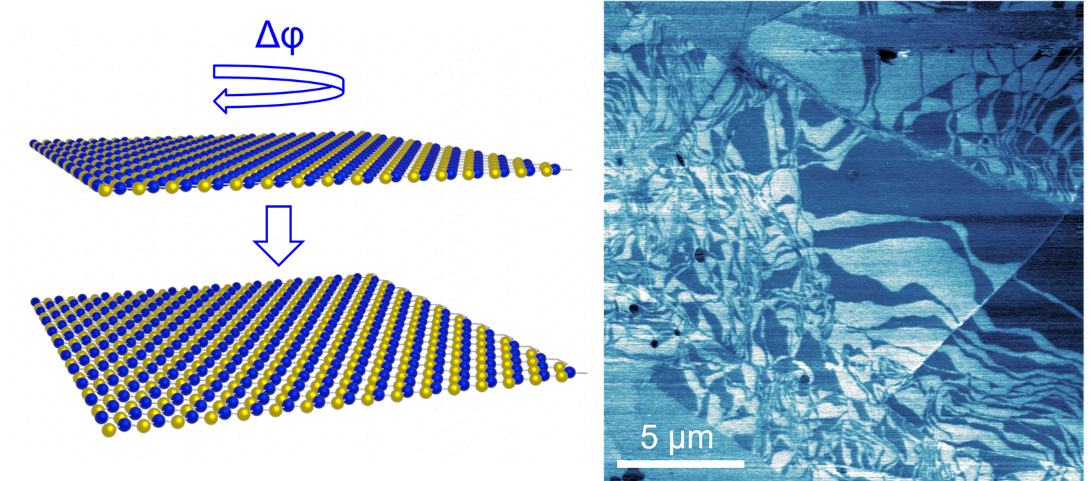
Ferroelectricity is observed in hexagonal boron nitride(hBN) through control of the registry of stacked layers, which we explore through both amplitude-modulated and sideband Kelvin probe force microscopy (KPFM) on the Park FX40 automatic AFM. A schematic of the formation of parallel stacked bilayer hBN is shown in addition to a contact potential difference map measured using sideband KPFM
However, this dual-pass mode has several technical drawbacks. First, due to the lift height the electrical signal measured by the tip is necessarily an averaged contribution of a larger area of the sample during second pass, which implies a loss in lateral resolution. Second, since the tip needs to scan each line twice, a longer image acquisition time must be considered. On the other hand, a simultaneous mechanical and electrical excitation of the lever at its resonant frequency would cause a severe crosstalk between topographic and electrical signals.
In Park Systems tools, we are currently implementing the new sideband KPFM mode, which allows for simultaneous imaging of the topography and surface potential with a high spatial potential resolution and improved sensitivity with respect to lift mode and other KPFM (e.g., off-resonance) methods. Here, the topography is detected at the resonance of the cantilever, while the electrical drive of the KPFM is applied at much lower frequencies between 1 and 4 kHz. Due to frequency mixing, satellite peaks or sidebands appear in 1 and 4 kHz from the resonance. The parallel detection of both excitations is feasible due to the presence of multiple lock-ins in the Park NX default electronics. Since the KPFM signal is detected on the sidebands and the topography is detected on the resonance, both signals can be measured simultaneously.
[1] U. Zerweck et al., Phys. Rev. B 71 (2005) 125424.
[2] A. Axt et al., Beilstein J. Nanotechnol. 9 (2018) 1809-1819.
[3] H. O. Jacobs et al., Ultramicroscopy 69 (1997) 39-49.

