The Latest Advances in AFM for Nanotechnology (CNS, Harvard Univ.)

In partnership with the Center for Nanoscale Systems, Park Systems is proud to announce a free workshop and live demo to take place on May 19, 2016 at Harvard University. The workshop will cover topics such as AFM automatizing software with Self-Optimizing Scan Control and Scanning Ion Conductance Microscopy (SICM) technology, both from Park Systems. In the subsequent live demo, Park Systems will also unveil the functionality of the Park NX10 SICM System—a tool designed to enable innovative studies in electrochemistry. The entire event is open to all interested parties and includes lunch.
l Event Date and Time : Thursday, May 19, 2016 from 10:00 AM to 2:00 PM
l Venue : Center for Nanoscale Systems, Harvard Univ., LISE 303 — 11 Oxford St., Cambridge, MA
Dr. Sang-il Park, Founder & CEO of Park Systems, will be a featured presenter at the event. His talk will cover continuous innovations at Park Systems including the revolutionary Park SmartScan software, a pioneering AFM intelligence that produces high quality images with only a single click.
 Dr.Sang-il Park
Chairman & CEO, Park Systems
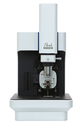
 Park NX10 SICM System
Event Agenda
l 10:00 AM — Event opening / Intro and Welcome (Dr. Arthur McClelland, Center for Nanoscale Systems)
l 10:30 AM — "Automatizing AFM using Self Optimizing Scan Control (Dr. Sang-il Park, Park Systems)
l 11:20 AM — Snack break / intermission
l 11:30 AM — "Park SICM Technology and its Applications" (Dr. Ardavan Zandiatashbar, Park Systems)
l 12:20 PM — Lunch
l 01:00 PM — Live Demo of Park NX10 SICM System
l 02:00 PM — Event closing
About Center for Nanoscale Systems
The Center for Nanoscale Systems (CNS) is a shared-use core facility at Harvard University. Our scientific focus is the study, design and fabrication of nanoscale structures and their integration into large and complex interacting systems.
At CNS, we help the Harvard and New England research community to create and study very small structures (from tens of microns down to a few atoms in width), and we enable these structures to be incorporated into very complex systems. Our users come from Harvard and other institutions across the country, and from start-ups and established corporations in nearly every field of endeavor.
Areas of current exploration at CNS: Photonics and Optical Computing, Biomimetics, Low-Temperature Physics, Graphene and other 2-D Materials, Diamond-based nano-scale sensors and computing elements, Photo-voltaics, Fuel-Cells, Energy Storage, and many more.
l Link : http://cns.fas.harvard.edu/
