-
Defect cannabinoid Dimethicone SPMLabs Conduct ScanningIon-ConductanceMicroscopy MeltingPoint I-VSpectroscopy DataStorage BreastCancerCell HydroGel BloodCell thermoplastic_elastomers molecular_self_assembly SSRM Lift fluoroalkane LightEmiting ElectrostaticForceMicroscopy Zhi LiBattery Silver Phase chemical_compound KelvinProbeForceMicroscopy Hole 3-hexylthiophene SiliconOxide MultiferroicMaterials StrontiuTitanate LFM atomic_steps Pinpoint Annealed Permalloy
Report image
If you found this image unacceptable, please let us know. We will review your report and take action if we determine this image is really unacceptable.
Trench Etch Profile on Si Wafer
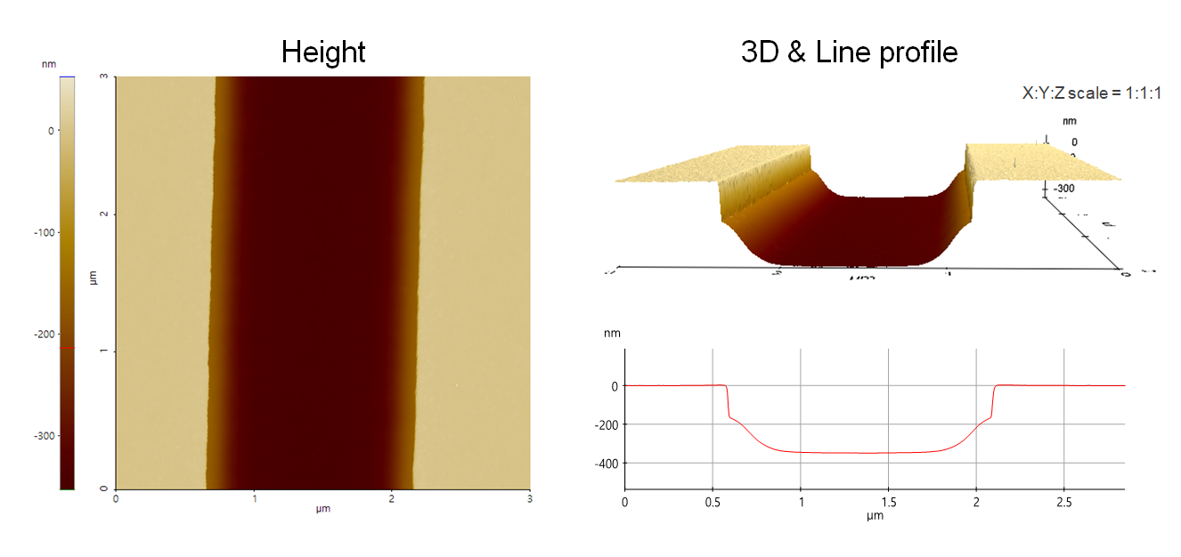
Top dielectric trench etch profile on Si wafer having tapered slope at the trench sidewall.
Scanning Conditions
- System: NX20
- Scan Mode: Non-contact
- Cantilever: AC160TS (k=26N/m, f=300kHz)
- Scan Size: 3μm×3μm
- Scan Rate: 0.21Hz
- Pixel: 1024 × 256
- Scan Mode: Non-contact
- Cantilever: AC160TS (k=26N/m, f=300kHz)
- Scan Size: 3μm×3μm
- Scan Rate: 0.21Hz
- Pixel: 1024 × 256