-
single_layer KPFM OrganicSemiconductor SRAM Current Tapping Vinylpyridine Galfenol fluorocarbon Heat Annealing Ucl ElectroDeposition piezoelectric force microscopy Solution hetero_structure MLCC PetruPoni_Institute Calcium dielectric trench Aggregated_molecules Adhesion KAIST Inorganic_Compound AAO Graphene Optical Praseodymium StainlessSteel alkanes Cobalt Tin sulfide SurfaceChange MagneticForceMicroscopy Sphere
Report image
If you found this image unacceptable, please let us know. We will review your report and take action if we determine this image is really unacceptable.
Taegeuk Mark Lithography on PZT
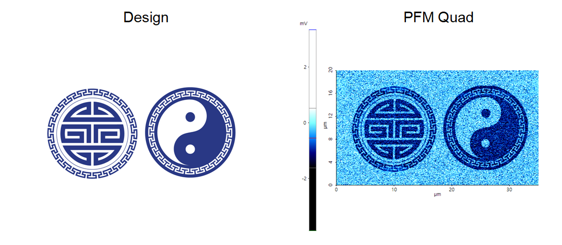
Re-arranged the domain pole direction on PZT surface using bias mode of lithography.
Scanning Conditions
- System: NX10
- Scan Mode: Lithography
- Cantilever: PPP-ContScPt (k=0.2N/m, f=25kHz)
- Scan Size: 35μm×20μm
- Scan Rate: 0.5Hz
- Pixel Size: 1024 × 1024
- Tip Bias: 10V for patterned area
- Scan Mode: Lithography
- Cantilever: PPP-ContScPt (k=0.2N/m, f=25kHz)
- Scan Size: 35μm×20μm
- Scan Rate: 0.5Hz
- Pixel Size: 1024 × 1024
- Tip Bias: 10V for patterned area