-
Scratch MonoLayer ItoGlass NCM DLaTGS molecular_beam Chungnam_National_University Tapping KelvinProbeForceMicroscopy light_emission Vortex STM Graphite EFMAmplitude GalliumPhosphide Iron CeNSE_IISc hard_disk Global_Comm Fet Bacterium Resistance Forevision C36H74 YszSubstrate plastic TemperatureControlledAFM Edwin PyroelectricDetector Molybdenum_disulfide Sapphire DataStorage Galfenol MechanicalProperty Imprint
Report image
If you found this image unacceptable, please let us know. We will review your report and take action if we determine this image is really unacceptable.
Ferroelectric superlattices in 2L-hBN (0°)
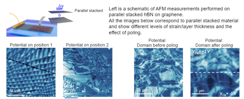
Scanning Conditions
- System : FX40
- Scan Mode: Sideband KPFM
- Scan Rate : All 0.3 Hz
- Scan Size : 3μm×3μm, 4μm×4μm
- Pixel Size : All 512×512
- Cantilever : ElectricMulti75-G (k=3N/m, f=75kHz)