-
ForceMapping Fluoride KelvinProbeForceMicroscopy SurfaceChange fluorocarbon Calcium MfmAmplitude FM_KPFM LFM PvdfFilm SRAM InsulatorFilm SiliconOxide Heating Phosphide 3-hexylthiophene Polytetrafluoroethylene PolymerBlend IcelandSpar Ecoli CBD CaMnO3 Conduct Filter ItoGlass PVA Hair SolarCell WPlug DeoxyribonucleicAcid hard_disk Wildtype CrAu amplitude_modulation CarbonNanotube
Report image
If you found this image unacceptable, please let us know. We will review your report and take action if we determine this image is really unacceptable.
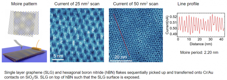
Graphene on hBN
Scanning Conditions
- System : FX40
- Sample bias: 1 V
- Scan Mode: C-AFM
- Scan Rate : 25 Hz for 25 nm2, 10 Hz for 50 nm2
- Scan Size : 25nm2×25nm2
- Pixel Size : 128×128 for 25 nm2, 256×256 for nm2
- Cantilever : ElectricMulti75-G (k=3N/m, f=75kHz)