Optimum Current Distribution Measurement of Zinc Oxide Nanorods via PinPoint™ Conductive AFM
Paul Pineda, Christina Newcomb, Gerald Pascual, Byong Kim, and Keibock Lee
Park Systems, 3040 Olcott Street, Santa Clara, CA 95054
ABSTRACT
The current distribution in a material is one of the significant parameters in determining the performance of electrical devices. As the components of these devices continue to miniaturize, measuring local properties have become more challenging to researchers and device engineers. Therefore, an advanced method that can provide an accurate and repeatable measurement in nanoscale level is of great importance. Conductive AFM (C-AFM) is uniquely suited to perform electrical measurements such as current distribution with nanoscale precision and can be performed in contact mode, tapping mode, or PinPoint™ mode. Here we perform C-AFM on ZnO nanorods, which have been widely studied due to their remarkable performance in electronics, optics, photonics, and photocatalysis. We compare traditional C-AFM performed in contact mode with tapping and Park’s proprietary PinPoint™ mode. We demonstrate that C-AFM in PinPoint™ mode provides information that correlates nanorod size to conductivity, which could not be obtained using C-AFM operating in the other modes. The advanced mechanism of this mode eliminates high frictional force and allows user to control the contact time and force, which enables high resolution imaging of the ZnO NRs.
INTRODUCTION
The discovery of Conductive Atomic Force Microscopy (C-AFM) in the mid 1990s has made a remarkable contribution in maintaining device reliability in various industries such as in semiconductor, solar cell, and hard disk drive manufacturing, among others [1,2]. The ever-shrinking dimensions of materials and devices in these industries have reached the limit of conventional test methods such that bulk property measurements can no longer describe their behavior. For this reason, the measurement of local properties of materials have become more effective over bulk property in providing accurate nano-scale measurement.
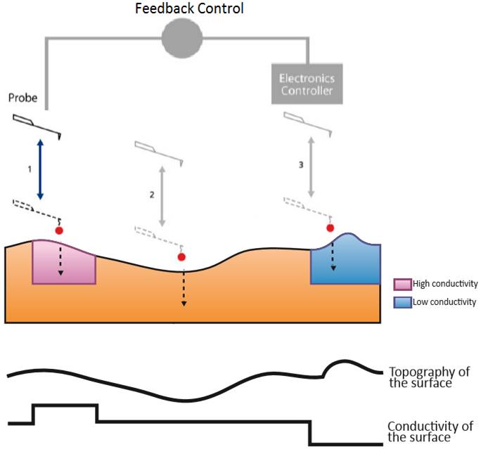
There are several methods that were introduced to measure these local properties, and the most common are scanning electron microscopes (SEMs) and focused ion beams (FIBs). [4] However, some of these techniques are destructive and others have a limited measurement and property characterization modes. One of the most powerful tools that was designed to overcome these problems is C-AFM. This technique provides both electrical properties and topography at the same time, first by monitoring the current flowing between the conductive tip and sample, and the latter by monitoring the cantilever deflection as the tip scans over the sample surface. However, the conventional C-AFM have some dis-advantages, examples include high frictional force due to continuous tip-sample contact resulting to quick tip wear and degradation of image resolution, and high signal-to-noise ratio. Another technique called Tapping mode was introduced to eliminate high frictional force. In this technique, the tip is oscillated near to its resonance frequency, allowing the tip to periodically touch the sample surface. But, this technique have limited tip pressure control and contact time resulting to lack of accuracy and precision measurements with relatively poor reproducibility of data. Recently, a new operational AFM mode developed by Park Systems called PinPoint™ can be coupled with C-AFM to offer research scientists and engineers an innovative solution to these problems. This method operates in an approach-retract manner, ensuring a frictionless operation which eliminates the lateral force due to continuous tip-sample contact (Figure 1). In addition, the contact time and contact force between the tip and sample surface are controllable, allowing acquisition of accurate and reproducible data even with soft samples, such as polymers. Here, we present the C-AFM results of the 3 techniques side by side using ZnO nanorods as standard.
ZnO NRs are widely used due to their unique electrical and optical properties. They are utilized in a electronics, optics, photonics, and photocatalysis. However, the electronic performance of these devices are often linked to the presence of surface defects and changes to the surface, which are not observable when performing bulk measurements. . A common example is the presence of adsorbates in ZnO NRs. Nanometer sized adsorbates can decrease the intrinsic conductivity of the materials. Another is the introduction of light irradiation to ZnO NRs. This change on surface condition leads to increase of surface conductivity. Therefore, a more sophisticated and precise method to validate the surface properties of materials is of great importance. Here we demonstrate that PinPoint™ Conductive AFM is the optimum method to measure the current distribution of a Zinc Oxide Nanorods (ZnO NRs), as it provides a controlled and frictionless measurement that allows the user to measure the topography and conductivity of a sample.
EXPERIMENTAL
A sample consisting of ZnO NRs was investigated using a Park NX10 AFM system. The sample’s topography and conductivity was measured under ambient air conditions to perform a 4 x 4 µm scan outputting to an image size of 256 x 256 px. Same sample was measured by three different C-AFM techniques in the following sequence: 1) PinPoint™ C-AFM, 2) contact C-AFM, and 3) tapping C-AFM. A conductive diamond coated probe (NANOSENSORS™ CDT-CONTR) with a nominal force constant of 0.5 N/m was utilized in the entire experiment.
In PinPoint™ C-AFM, the sample’s topography and electrical properties (such as conductivity) can be acquired simultaneously. The conductive tip maps the topography by monitoring its feedback signal, approaching the sample until it reaches a predefined threshold point, measuring Z scanner height, and rapidly retracts. The threshold point that was applied to the sample was set to 100 mV while the control height setting, which is equivalent to the magnitude of retraction, was set to 0.5 um since the baseline used in this mode was established by using these values. The current distribution of the samples are mapped each time the tip engages the sample surface. The current flow produced by the application of a bias voltage between the conductive tip and sample is measured at each landing point to acquire the electrical data. Generally, the current flow is very small and needs to be amplified by a current amplifier before it can be processed into an image. The Park NX10 is equipped with internal current amplifier with variable gain of 106~1012 V/A which is applicable to most measuremens. The applied external sample bias that was used in the experiment was 3V. In data acquisition, the XY scanner stops, and the contact time is controlled to give enough time for the scanner to acquire precise and accurate data. The contact time that was used in this experiment is 4 ms. This entire process is repeated for each pixel in the target scan image until the image is completed [7].

Figure 1. Principles of PinPoint™ Conductive AFM. This diagram demonstrates the feedback-controlled approach and retraction of a C-AFM probe at multiple sites along a sample’s surface. Feedback control from the AFM system’s controller allows this technique to acquire both surface topography and conductivity data as in traditional C-AFM and tapping C-AFM, but without thedrawbacks.
RESULTS AND DISCUSSION
Topography Data
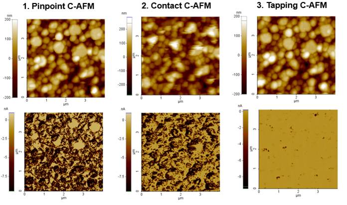
The topography data measured using the three techniques are shown in Figure a-c. The images revealed that the scanned area of the sample is composed of tendril-like structures that are grouped together pointing in an upright position. The cross sectional shape of each individual NRs are observed to have hexagonal shape with diameters that vary from 200 to 800 nm and heights that range from 30 to 200 nm. The topography data measured by contact C-AFM has poor quality compared to PinPoint™ C-AFM and tapping C-AFM due to lower spatial resolution and artifacts visible in some areas of the image. Such quality can be attributed to continuous tip-sample contact that produces high frictional force leading to damage of both the tip and the sample, and low signal-to noise ratio that intensively degrades the accuracy of the acquired measurement.
Current Distribution
The current distribution of the sample shown in figures e-f was mapped by using a color table in XEI, an image analysis software developed by Park Systems. The intensity of the shading correlates to the degree of surface conductivity. In this experiment, the darker regions represents a higher surface conductivity while lighter regions represents a lower surface conductivity. The absolute value of the current for an individual NR ranges from 0 to 9 nA. By comparing the results of the three techniques, one can easily determine that PinPoint™ C-AFM is the most sensitive method in detecting local conductivity variations as the current data acquired in this mode detects significant differences in the conductive regions. The images acquired using the other modes (contact mode and tapping mode) show less conductivity with fewer features. Shorter contact time during the measurement may contribute to the poor image quality. The data acquired using PinPoint™ mode provides unique insight into the electrical properties of the sample. For example, the ZnO NRs with smaller diameters are more conductive compared to those with larger diameters. Such an interpretation would not be realized by performing either of the other two techniques.

Figure 1. 1.) Data acquired using PinPoint™ C-AFM (Topography: a, Current: d) 2.) Data acquired using Contact C-AFM (Topography: b, Current: e), and 3.) Data acquired using Tapping C-AFM (Topography: c, Current data: f). Scan size: 4 x 4 µm, image size: 256 x 256 px.
CONCLUSIONS
Among the techniques reported here, PinPoint™ C-AFM developed by Park Systems provides the best quality of data for both topography and current measurements. The advanced mechanism of this mode eliminates high frictional force which enables high resolution imaging of the ZnO NRs. The structure of the sample was clearly observed to have a hexagonal cross-section with diameters ranging from 200 to 800 nm and heights from 30 to 200 nm. Furthermore, its ability to control the contact force and time allows accurate mapping of the current variations in the surface. In this study, the ZnO NRs with smaller diameters were observed to be more conductive compared to those with larger diameters. Given the above results, C-AFM is the optimum method that can be used to measure sample’s topography and current distribution simultaneously at nanoscale, without sacrificing the tip and sample quality, and the accuracy of measurements.
REFERENCES
[1] I Gromyko, et al., ZnO Nanorods Grown Electrochemically on Different Metal Oxide Underlays, IOP Conf. Series: Materials Science and Engineering.
[2] C. Teichert, et al., Conductive Atomic-Force Microscopy Investigation of Nanostructures in Microelectronics.
[3] K. Bandopadhyay, et al., Spatially resolved photoresponse on individual ZnO nanorods: correlating morphology, defects and conductivity
[4] K. Lee, Failure analysis and the innovative PinPoint™ conductive AFM
[5] http://www.parkafm.com/index.php/park-afm-modes/electrical-modes?i=1
[6] http://www.parkafm.com/index.php/park-spm-modes/94-electrical-properties/233-conductive-afm
