-
Fet Typhimurium Lattice neodymium_magnets IRDetector ThinFilm MeltingPoint Copper PVA light_emitting ImideMonomer KelvinProbeForceMicroscopy domain_switching hard_disk UnivMaryland multi_layer LogAmplifier Adhesion Metal Ceramics Al2O3 #EC CrossSection SiliconeOxide MolecularSelfAssembly RedBloodCell Austenite Piezo FailureAnlaysis Floppy CrystalGrowing Scanning_Thermal_Microscopy Hexylthiophene PS_PVAC Piezoresponse
Report image
If you found this image unacceptable, please let us know. We will review your report and take action if we determine this image is really unacceptable.
MoS2 Layers on SiO2
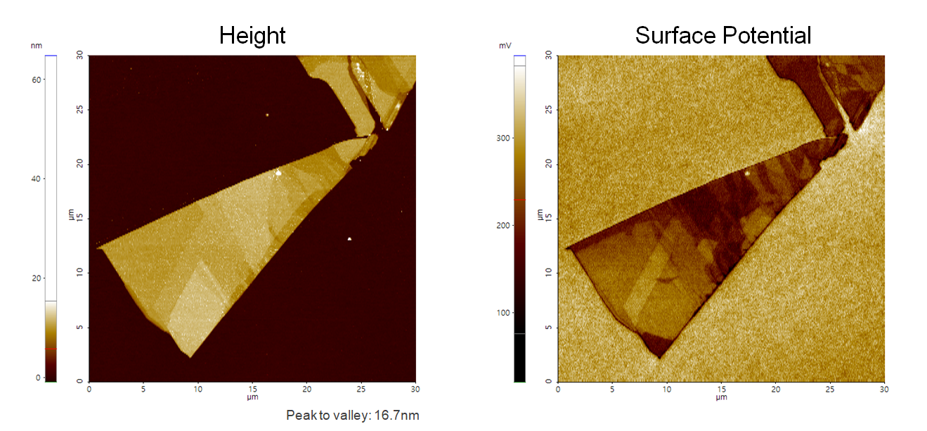
A few layers of MoS2 on SiO2
Scanning Conditions
- System: NX10
- Scan Mode: AM-KPFM
- Cantilever: NSC36Cr-Au B (k=2N/m, f=130kHz)
- Scan Size: 30μm×30μm
- Scan Rate: 0.3Hz
- Pixel Size: 512 × 256
- Scan Mode: AM-KPFM
- Cantilever: NSC36Cr-Au B (k=2N/m, f=130kHz)
- Scan Size: 30μm×30μm
- Scan Rate: 0.3Hz
- Pixel Size: 512 × 256