-
FuelCell BaTiO3 solar_cell Ni-FeAlloy UnivCollegeLondon Plug LeakageCurrent StyreneBeads Jason Trench self_healing CNT Gallium cannabinoid PS_PVAC LiquidCell Led SSRM SicMosfet Polyethylene Film CrAu Morphology dielectric trench INSPParis ferromagnetic PVAP3HT Conductance Gong graphene_hybrid AAO FAPbI3 GaP Sic Thermal
Report image
If you found this image unacceptable, please let us know. We will review your report and take action if we determine this image is really unacceptable.
Monolayer Graphene on PDMS Surface
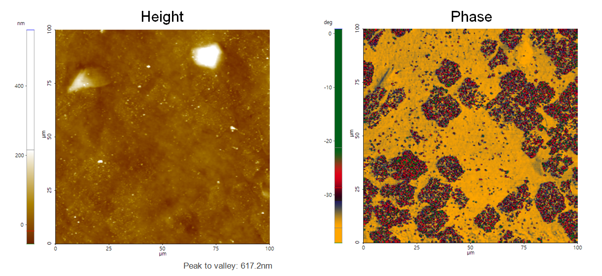
Monolayer Graphene grown on Cu foil using CVD process is transferred on to PDMS substrate.
Scanning Conditions
- System: NX20
- Scan Mode: Tapping
- Cantilever: Access-NC (k=113N/m, f=330kHz)
- Scan Size: 100μm×100μm
- Scan Rate: 0.6Hz
- Pixel Size: 256 × 256
- Scan Mode: Tapping
- Cantilever: Access-NC (k=113N/m, f=330kHz)
- Scan Size: 100μm×100μm
- Scan Rate: 0.6Hz
- Pixel Size: 256 × 256