-
atomic_steps ImideMonomer Lateral IRDetector Temperature Ucl Graphite sputter BariumTitanate Topography PolyvinylideneFluoride Nanofiber HighResolution MoirePattern SetpointMode Water HexagonalBoronNitride ScanningThermalMicroscopy Photovoltaics Blend molecule GaAs thermal_conductivity Indium_tin_oxide ScanningIon-ConductanceMicroscopy OxideLayer HafniumDioxide LifeScience Boundary Granada strontiu_titanate Reading nanobar Styrene HydroGel
Report image
If you found this image unacceptable, please let us know. We will review your report and take action if we determine this image is really unacceptable.
PS/LPDE
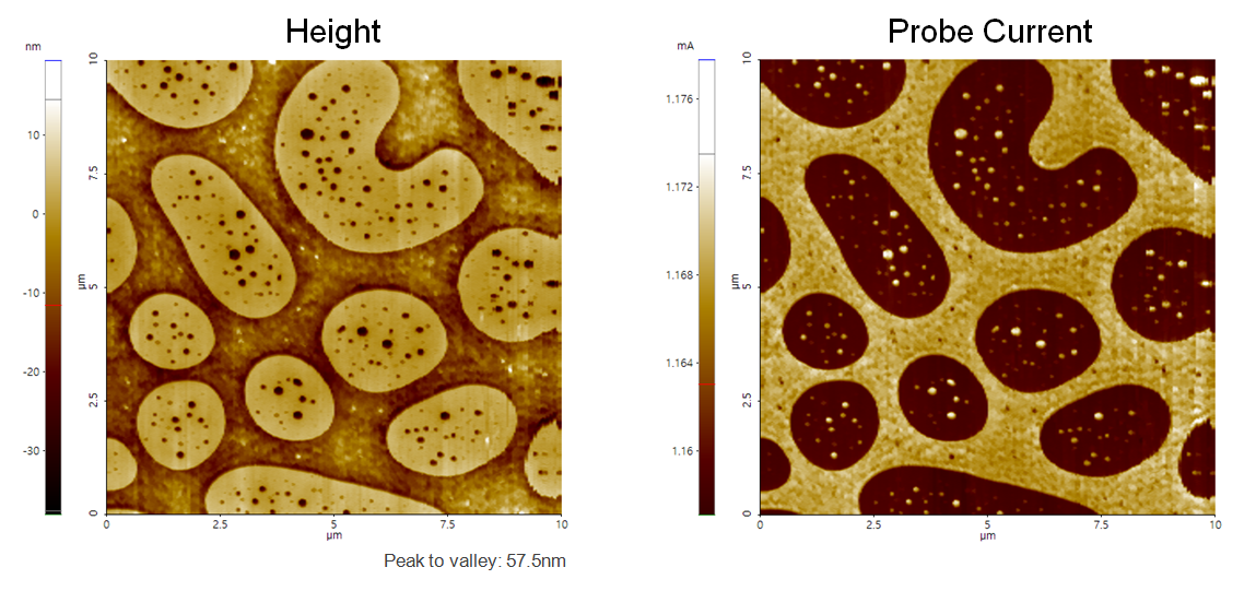
Spincast layer of PS/LDPE blend on Si. Signal change by thermal conductivity difference.
Scanning Conditions
- System: NX10
- Scan Mode: SThM
- Cantilever: NanoThermal Probe
- Scan Size: 10μm×10μm
- Scan Rate: 0.5Hz
- Pixel Size: 256 × 512
- Scan Mode: SThM
- Cantilever: NanoThermal Probe
- Scan Size: 10μm×10μm
- Scan Rate: 0.5Hz
- Pixel Size: 256 × 512