-
Sic PANI PolycrystallineFerroelectricBCZT Mosfet GalliumPhosphide Trench ElectrostaticForceMicroscopy StrontiumTitanate Carbon phase_change CuParticle MagneticPhase Alkane PhaseTransition gallium_nitride Inorganic FloppyDisk Optoelectronic Tape conductive Zagreb ForceMapping Polyethylene SPMLabs Calcium SrTiO3 HOPG Edwin HumanHair SetpointMode Permalloy OpticalElement Electrode Liquid Polyimide
Report image
If you found this image unacceptable, please let us know. We will review your report and take action if we determine this image is really unacceptable.
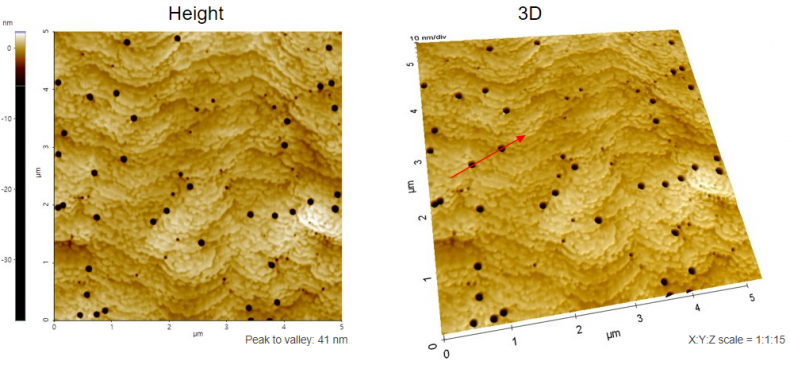
GaN epi wafer

Scanning Conditions
- System : NX-Wafer
- Scan Mode: Non-contact
- Scan Rate : 0.7 Hz
- Scan Size : 5μm×5μm
- Pixel Size : 512×512
- Cantilever : PPP-NCHR (k=42N/m, f=330kHz)
