-
BiasMode UnivMaryland FAPbI3 single_layer UTEM Crystal optoelectronics HACrystal Mechanical NCM\ TungstenThinFilmDeposition Hydroxyapatite temperature controller AFM HumanHair Carbon hard_disk_media biocompatible Al2O3 Solution Electronics Roughness ThermalConductivity CancerCell Ito Silver Water Resistance Edwin Polymer Phosphide PrCurve epitaxy MolecularSelfAssembly LDPE Organic
Report image
If you found this image unacceptable, please let us know. We will review your report and take action if we determine this image is really unacceptable.
Multi-layer necking device defect
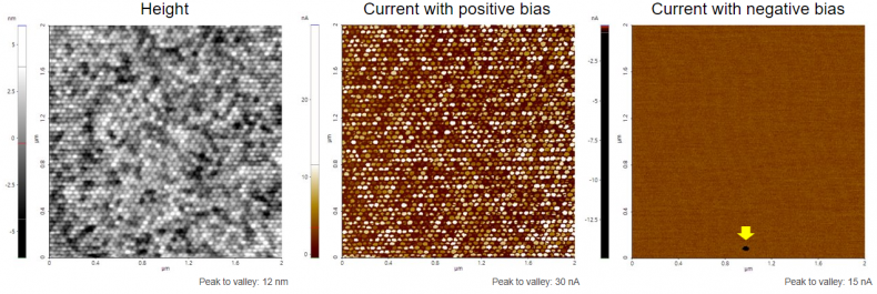
Scanning Conditions
- System : NX-Wafer
- Scan Mode: C-AFM
- Scan Rate : 2Hz
- Scan Size : 2μm×2μm
- Pixel Size : 512×256
- Cantilever : AD-2.8-AS (k=2.8N/m, f=75kHz)