-
Aluminum Pattern Magnetostrictive FrequencyModulation Genetic Aluminium_Oxide DLaTGS Trench PMNPT semifluorinated_alkanes ScanningIon-ConductanceMicroscopy PtfeFilter GalliumPhosphide PFM Tape Force-distance FailureAnlaysis Floppy BaTiO3 Phosphide Pzt StainlessSteel InLiquid Ni-FeAlloy Foil KevlarFiber MechanicalProperty fe_nd_b hetero_structure PDMS lift_mode membrane optoelectronics Molybdenum_disulfide Carbon
Report image
If you found this image unacceptable, please let us know. We will review your report and take action if we determine this image is really unacceptable.
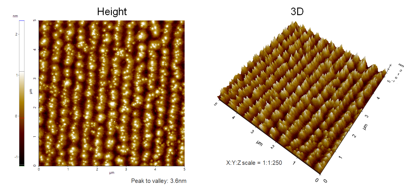
AlN/GaN/AlN Hetero Structure

AlN/GaN/AlN hetero structure grown on SiC substrate by Molecular Beam Epitaxy (MBE) system.
Scanning Conditions
- System: NX20
- Scan Mode: Non-contact
- Cantilever: AC160TS (k=26N/m, f=300kHz)
- Scan Size: 5μm×5μm
- Scan Rate: 0.5Hz
- Pixel Size: 512 × 512
- Scan Mode: Non-contact
- Cantilever: AC160TS (k=26N/m, f=300kHz)
- Scan Size: 5μm×5μm
- Scan Rate: 0.5Hz
- Pixel Size: 512 × 512
