-
ring shape multi_layer Gallium_Arsenide Indium_tin_oxide STO Floppy AAO Polymer Conductive AFM SingleLayer OxideLayer Foil LightEmission ShenYang Moire molecule PinpointPFM Singapore plastics ElectroDeposition TemperatureControlledAFM hard_disk InsulatorFilm ForceMapping Cancer Styrene MeltingPoint ThermalDetectors SicMosfet GaN MESA structure Alkane SAM UnivCollegeLondon Strontium
Report image
If you found this image unacceptable, please let us know. We will review your report and take action if we determine this image is really unacceptable.
Trench Etch Profile on MESA
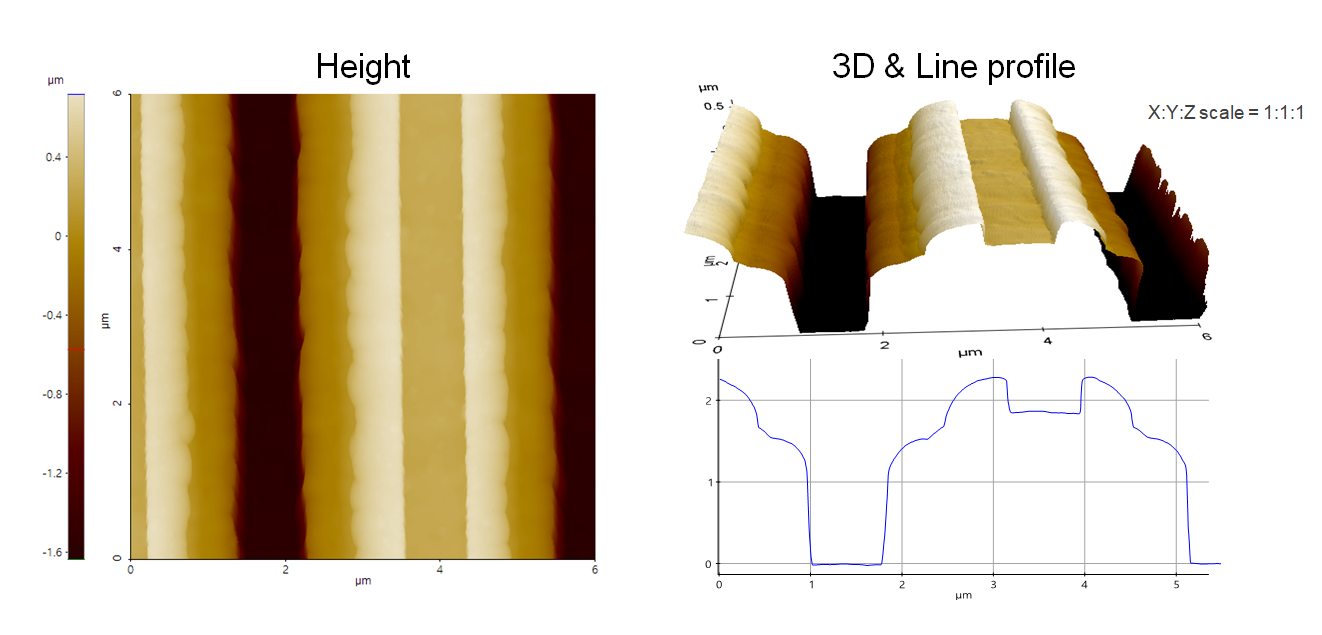
Top dielectric trench etch profile on MESA on Si wafer.
Scanning Conditions
- System: NX20
- Scan Mode: Non-contact
- Cantilever: AR5T-NCHR (k=42N/m, f=300kHz)
- Scan Size: 6μm×6μm
- Scan Rate: 0.12Hz
- Pixel Size: 1024 × 256
- Scan Mode: Non-contact
- Cantilever: AR5T-NCHR (k=42N/m, f=300kHz)
- Scan Size: 6μm×6μm
- Scan Rate: 0.12Hz
- Pixel Size: 1024 × 256