-
semifluorinated alkane Cancer Polypropylene F14H20 IRDetector Water PolymerBlend DiffractiveOpticalElements Genetic LaAlO3 Vanadate Implant AAO PhaseTransition LogAmplifier PolymerPatterns OpticalWaveguide MembraneFilter Pyroelectric SolarCell Floppy ContactMode FrictionForce Sadowski PhthalocyaninePraseodymium Ni-FeAlloy Dimethicone EPFL Pzt StyreneBeads PtfeMembrane SurfaceChange Scanning_Thermal_Microscopy SetpointMode Bacteria
Report image
If you found this image unacceptable, please let us know. We will review your report and take action if we determine this image is really unacceptable.
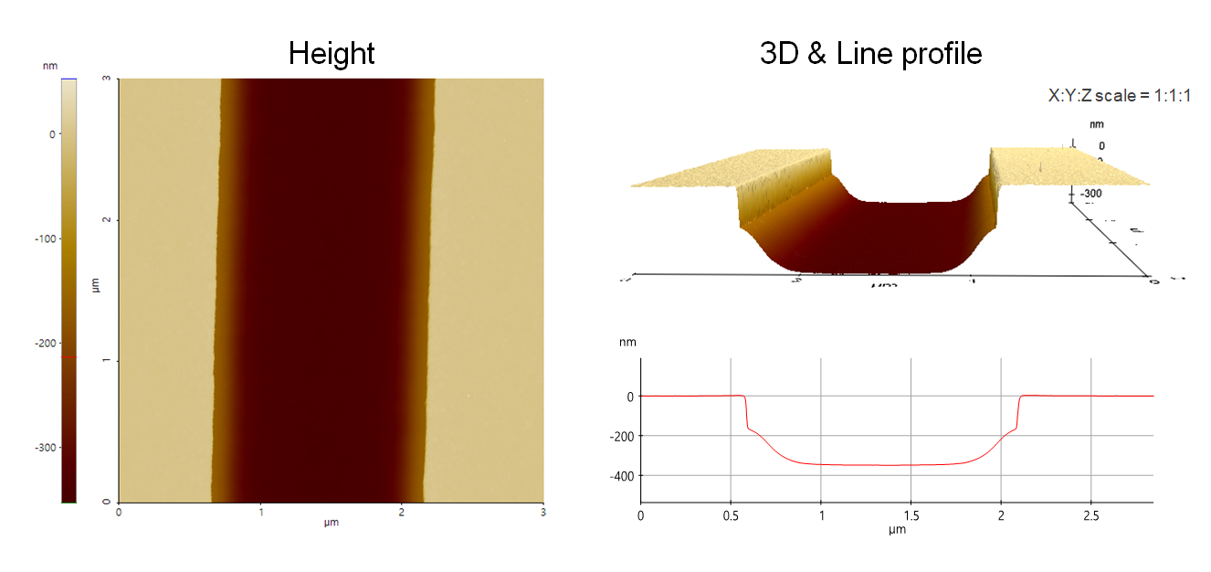
Trench Etch Profile on Si Wafer

Top dielectric trench etch profile on Si wafer having tapered slope at the trench sidewall.
Scanning Conditions
- System: NX20
- Scan Mode: Non-contact
- Cantilever: AC160TS (k=26N/m, f=300kHz)
- Scan Size: 3μm×3μm
- Scan Rate: 0.21Hz
- Pixel: 1024 × 256
- Scan Mode: Non-contact
- Cantilever: AC160TS (k=26N/m, f=300kHz)
- Scan Size: 3μm×3μm
- Scan Rate: 0.21Hz
- Pixel: 1024 × 256
