-
lithography Heat BlockCopolymer Vanadate LiquidImaging medical DeoxyribonucleicAcid PVAP3HT ContactModeDots FailureAnalysis semifluorinated_alkane ScanningSpreadingResistanceMicroscopy CalciumHydroxyapatite Electrode Tapping Vinylpyridine LiquidCrystal Step ElectrostaticForceMicroscopy Scanning_Thermal_Microscopy SurfaceChange LightEmiting Anneal FuelCell strontiu_titanate GaAs CopperFoil Nanofiber Formamidinium_lead_iodide Chrome FM-KPFM Magnets PetruPoni phase_change Hexacontane
Report image
If you found this image unacceptable, please let us know. We will review your report and take action if we determine this image is really unacceptable.
MoS2 Layers on SiO2
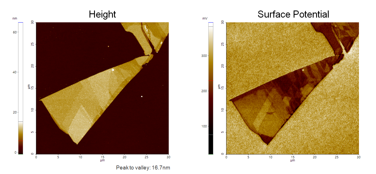
A few layers of MoS2 on SiO2
Scanning Conditions
- System: NX10
- Scan Mode: AM-KPFM
- Cantilever: NSC36Cr-Au B (k=2N/m, f=130kHz)
- Scan Size: 30μm×30μm
- Scan Rate: 0.3Hz
- Pixel Size: 512 × 256
- Scan Mode: AM-KPFM
- Cantilever: NSC36Cr-Au B (k=2N/m, f=130kHz)
- Scan Size: 30μm×30μm
- Scan Rate: 0.3Hz
- Pixel Size: 512 × 256