-
CaMnO3 Step SmallScan Polyvinylidene_fluoride TemperatureControl Friction self-assembled_monolayer LDPE Logo Gong AdhesionForce InsulatorFilm epitaxy EFM LiIonBattery NUS_NNI_Nanocore BreastCancerCell Wildtype FM_KPFM ForceVolumeImage Optical China F14H20 VortexCore KevlarFiber Bismuth Inorganic KAIST TemperatureControllerAFM StainlessSteel Mechanical CrAu Pores bias_mode IISCBangalore
Report image
If you found this image unacceptable, please let us know. We will review your report and take action if we determine this image is really unacceptable.
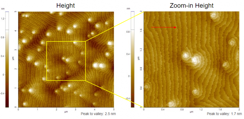
GaN on Si epi film

Scanning Conditions
- System : NX20
- Scan Mode: Non-contact
- Scan Rate : All 2 Hz
- Scan Size : 5µm2, 5µm2
- Pixel Size : ALL 512×512
- Cantilever : OMCL-AC160TS (k=26N/m, f=300kHz)
