-
Austenite Moire Self-assembledMonolayer TriGlycineSulphate LiquidCrystal hetero_structure NUS_Physics CBD SelfAssembly PDMS Cancer PVA Organic SolarCell ferromagnetic Semiconductor SiliconOxide cannabis PMNPT HafniumDioxide Chemical_Vapor_Deposition sputter AM_KPFM Mechanical Patterns HexagonalBN Mfm Annealed pinpoint mode molecule Floppy Hafnia Optic Array PhaseTransition
Report image
If you found this image unacceptable, please let us know. We will review your report and take action if we determine this image is really unacceptable.
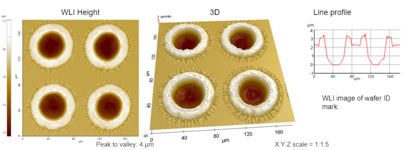
WLI image of wafer ID mark

Scanning Conditions
- System : NX-Hybrid WLI
- Scan Mode: WLI
- Field of view: 182μm×182μm
