-
GlassTemp DIWafer LogAmplifier Fet Polyimide Silver NtuEee Yeditepe conductive BCZT ForceVolumeImage atomic_layer HighResolution HexagonalBoronNitride Collagen FailureAnalysis Vacuum Optic ForceDistanceSpectroscopy thermal_property DentalProsthesis Indium_tin_oxide Battery cross section SurfaceChange Mechanical Formamidinium_lead_iodide Epoxy Beads Mfm HafniumDioxide CaMnO3 Biofilm ForceMapping BiFeO3
Report image
If you found this image unacceptable, please let us know. We will review your report and take action if we determine this image is really unacceptable.
Photoresist pattern (post-development process)
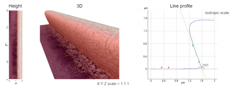
Scanning Conditions
- System : NX-3DM
- Scan Mode: Non-contact
- Scan Rate : 0.1 Hz
- Scan Size : 2μm×10μm
- Pixel Size : 512×2048
- Cantilever : EBD-R2-NCLR (k=45N/m, f=190kHz)