-
Mosfet HBN CeramicCapacitor Ucl Modulus FailureAnlaysis Formamidinium_lead_iodide Tin sulfide VerticalPFM Copolymer NusEce BiVO4 Beads FastScan Permalloy VortexCore Dopped Cancer Oxidation OpticalElement Array Battery Conduct Chemical_Vapor_Deposition HexagonalBoronNitride lithography FuelCell Defects Celebration Ram Scanning_Thermal_Microscopy BFO phase_change Piezoresponse HighAcpectRatio
Report image
If you found this image unacceptable, please let us know. We will review your report and take action if we determine this image is really unacceptable.
MoSi₂ Hard defect repair
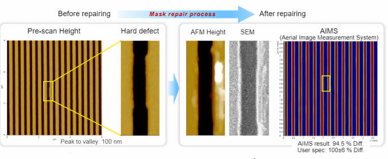
Scanning Conditions
- System : NX-Mask
- Scan Mode: Non-contact for imaging Sweep for repairing
- Scan Rate : 0.3 Hz
- Scan Size : 6μm, 0.5μm×1μm
- Pixel Size : 512×64 for 6μm2, 512×34 for 0.5μm×1μm