-
Water Blend GaN NTU PECurve Sadowski Piezoresponse Ferrite Gold Korea hetero_structure Cross-section University_of_Regensburg Grain TungstenThinFilmDeposition PpLdpe Hydroxyapatite heterojunctions molecular_beam Iron Fujian FM_KPFM SingleLayer StrontiuTitanate LiBattery Fiber CompactDisk LiftMode Hafnia Mechanical&nanotechnology SFAs MoirePattern Neodymium epitaxy BismuthVanadate
Report image
If you found this image unacceptable, please let us know. We will review your report and take action if we determine this image is really unacceptable.
Hard defect repair of photomask
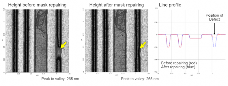
Scanning Conditions
- System : NX-Mask
- Scan Mode: Non-contact for imaging Sweep for repairing
- Scan Rate : 0.3 Hz
- Scan Size : 1.25μm×1.25μm
- Pixel Size : 256×256
- Cantilever : OMCL-AC160TS for imaging, AD-40 AS for repairing (k=42N/m, f=330kHz)