-
SRAM Optoelectronic medical mfm_amplitude PolymerBlend Praseodymium CuFoil Fluoride PANI HexagonalBN FM_KPFM Cell Growing norganic InLiquid SiliconOxide IISCBangalore Insulator FastScan HDD temperature controller AFM University_of_Regensburg Molybdenum_disulfide Patterns gallium_nitride UnivOfMaryland Techcomp Thermoplastic_polyurethane Semiconductor StainlessSteel ULCA AlkaneFilm fe_nd_b SrTiO3 LFM
Report image
If you found this image unacceptable, please let us know. We will review your report and take action if we determine this image is really unacceptable.
Multi-layer necking device defect
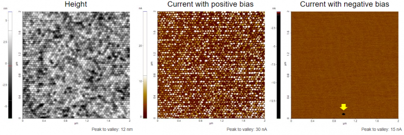
Scanning Conditions
- System : NX-Wafer
- Scan Mode: C-AFM
- Scan Rate : 2Hz
- Scan Size : 2μm×2μm
- Pixel Size : 512×256
- Cantilever : AD-2.8-AS (k=2.8N/m, f=75kHz)