-
Singapore Chemical_Vapor_Deposition BariumTitanate MechanicalProperty tip_bias_mode MembraneFilter Temasek_Lab Gong Electical&Electronics HexacontaneFilm Reading Ni-FeAlloy Hair StrontiuTitanate Laser NanoLithography Defect Tapping Wonseok bias_mode Vortex LightEmiting Polytetrafluoroethylene Fluoride SrO Hexylthiophene MfmAmplitude atomic_steps BiVO4 TemperatureControlledAFM Patterns Pinpoint PFM Plug PhaseTransition TempControl
Report image
If you found this image unacceptable, please let us know. We will review your report and take action if we determine this image is really unacceptable.
SiC MOSFET
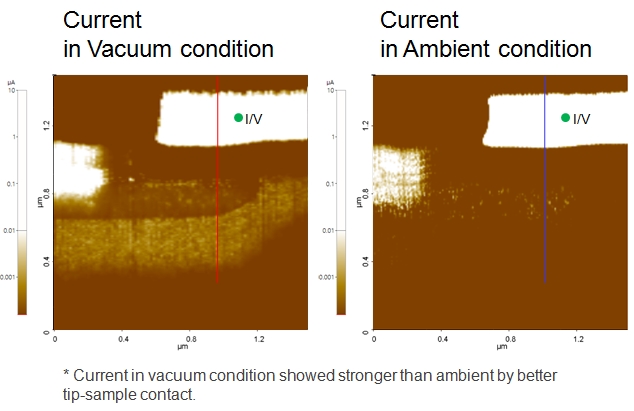
Scanning Conditions
- System: NX-Hivac
- Scan Mode: SSRM
- Cantilever: Full diamond (k=27 N/m)
- Scan Size: 2μm×2μm
- Scan Rate: 0.5Hz
- Pixel: 256×512
- Sample Bias: +2.5V
- Scan Mode: SSRM
- Cantilever: Full diamond (k=27 N/m)
- Scan Size: 2μm×2μm
- Scan Rate: 0.5Hz
- Pixel: 256×512
- Sample Bias: +2.5V