-
Pores Topography Non-ContactMode FrequencyModulation LaAlO3 Aluminum China Filter Composition OxideLayer Conducting PECurve HumanHair Au111 Reduction MfmPhase 3-hexylthiophene DIWafer Pipette SThM Fet Foil sputter Metal-organicComplex PVAC biocompatible PetruPoni PhthalocyaninePraseodymium Chromium mono_layer ScanningKelvinProbeMicroscopy UnivOfMaryland Ferroelectric BlockCopolymer NUS_Physics
Report image
If you found this image unacceptable, please let us know. We will review your report and take action if we determine this image is really unacceptable.
Atomic steps on GaP(Gallium Phosphide) layer on Si
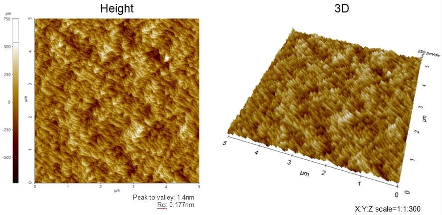
Scanning Conditions
- System: NX20
- Scan Mode: Non-contact
- Cantilever: PPP-NCHR (k=42N/m, f=300kHz)
- Scan Size: 5μm×5μm
- Scan Rate: 1Hz
- Pixel: 512×512