-
Lanthanum_aluminate Tungsten Growth Temasek_Lab Tape ForceDistanceSpectroscopy PolycrystallineFerroelectricBCZT Fiber Ucl CuSubstrate Modulus Dr.JurekSadowski INSPParis Boundary Forevision ReflexLens Wafer ThinFilm F14H20 Christmas Holes Au111 Metal NtuEee HOPG polyvinyl acetate fluoroaalkane Phenanthrene SolarCell CHRYSALIS_INC HighAspect ring shape Copolymer Varistor Lateral
Report image
If you found this image unacceptable, please let us know. We will review your report and take action if we determine this image is really unacceptable.
Polymer (1/2)
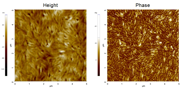
Scanning Conditions
- System: NX10
- Scan Mode: Tapping
- Cantilever: AC160TS
- Scan Size: 5μm×5μm
- Scan Rate: 0.5Hz
- Pixel: 512×512
- Scan Mode: Tapping
- Cantilever: AC160TS
- Scan Size: 5μm×5μm
- Scan Rate: 0.5Hz
- Pixel: 512×512