-
TungstenThinFilmDeposition sputter conductive LiBattery ito_film SrO PolyvinylAcetate fluoroalkane Dr.JurekSadowski dielectric trench Cancer ScanningIon-ConductanceMicroscopy Filter BloodCell HexagonalBoronNitride thermal_property silicon_oxide Pore MfmAmplitude high_resolution LiquidCell CBD H-BN Oxidation SoftSample TransitionMetal TemperatureControlledAFM CHRYSALIS_INC Au111 polyvinyl acetate graphene_hybrid Logo semifluorinated_alkane Croatia Gallium_Arsenide
Report image
If you found this image unacceptable, please let us know. We will review your report and take action if we determine this image is really unacceptable.
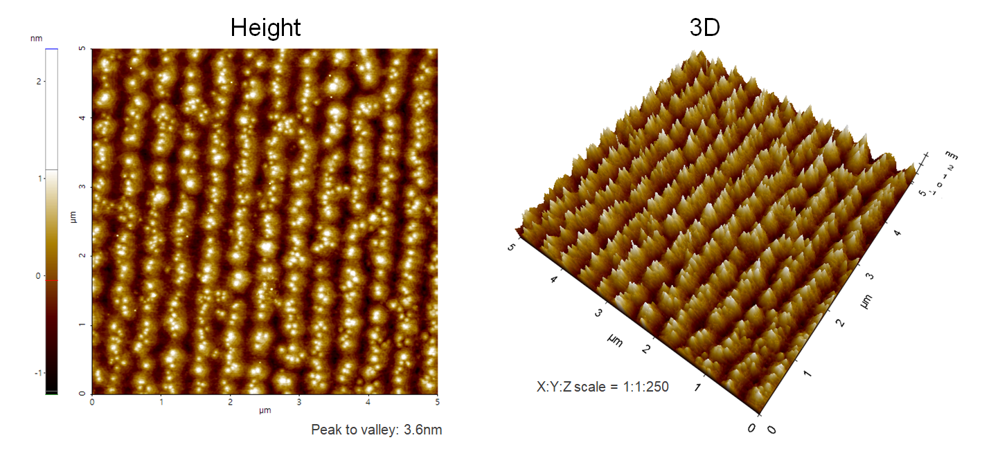
AlN/GaN/AlN Hetero Structure

AlN/GaN/AlN hetero structure grown on SiC substrate by Molecular Beam Epitaxy (MBE) system.
Scanning Conditions
- System: NX20
- Scan Mode: Non-contact
- Cantilever: AC160TS (k=26N/m, f=300kHz)
- Scan Size: 5μm×5μm
- Scan Rate: 0.5Hz
- Pixel Size: 512 × 512
- Scan Mode: Non-contact
- Cantilever: AC160TS (k=26N/m, f=300kHz)
- Scan Size: 5μm×5μm
- Scan Rate: 0.5Hz
- Pixel Size: 512 × 512
