-
alkanes hetero_structure Galfenol Force-distance SelfAssembly Wang molecular_beam amplitude_modulation AEAPDES Gallium_Arsenide Electronics Current CopperFoil MolecularSelfAssembly PrCurve fluorocarbon Subhajjit AdhesionEnergy silicon_carbide OpticalElement Nanotechnology Hexacontane Sio2 mechanical_property Sidewall Indium_tin_oxide PolycrystallineFerroelectricBCZT Al2O3 Polystyrene non_contact SmalScan ScanningKelvinProbeMicroscopy CntFilm Cobalt-dopedIronOxide DiffractiveOpticalElements
Report image
If you found this image unacceptable, please let us know. We will review your report and take action if we determine this image is really unacceptable.
MoS2 Layers on SiO2
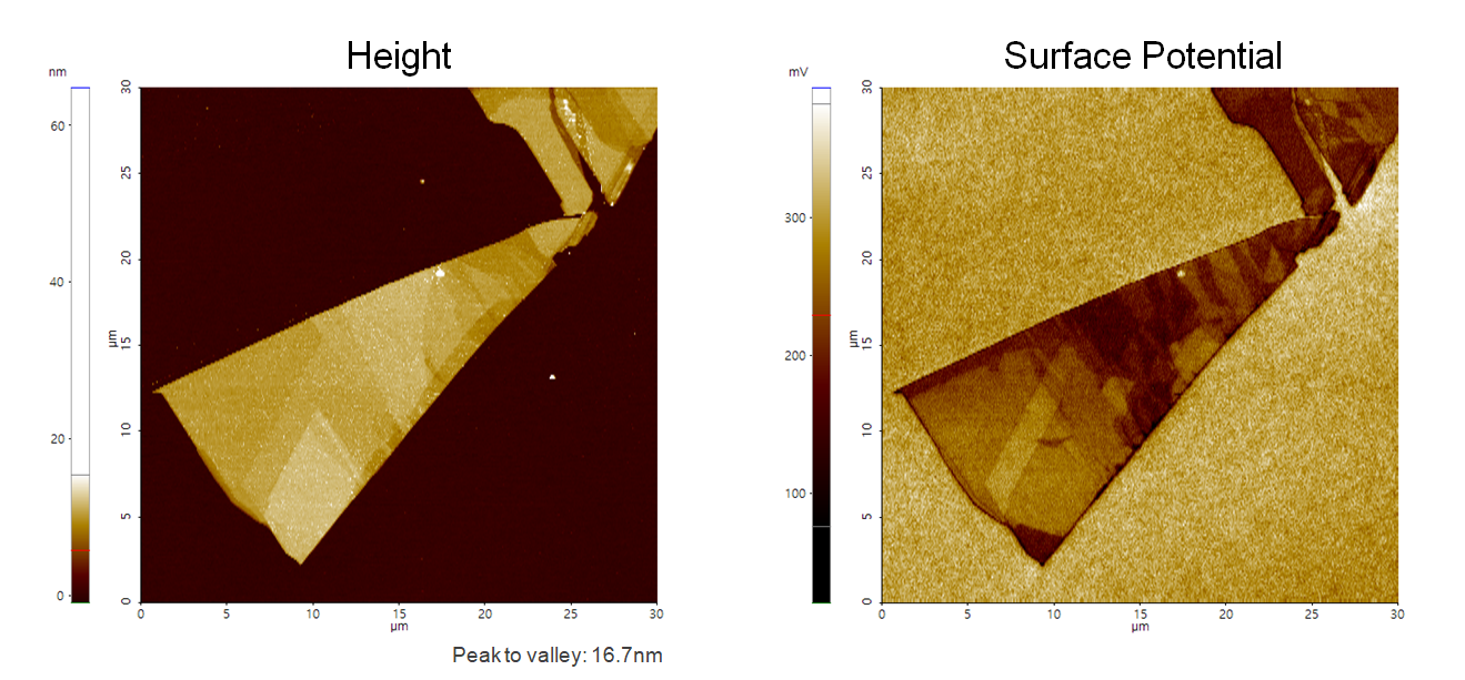
A few layers of MoS2 on SiO2
Scanning Conditions
- System: NX10
- Scan Mode: AM-KPFM
- Cantilever: NSC36Cr-Au B (k=2N/m, f=130kHz)
- Scan Size: 30μm×30μm
- Scan Rate: 0.3Hz
- Pixel Size: 512 × 256
- Scan Mode: AM-KPFM
- Cantilever: NSC36Cr-Au B (k=2N/m, f=130kHz)
- Scan Size: 30μm×30μm
- Scan Rate: 0.3Hz
- Pixel Size: 512 × 256