-
HumanHair PolymerPatterns ThermalConductivity PhaseImaging SurfaceChange LiquidCrystal DomainSwitching Mfm ScanningIon-ConductanceMicroscopy CNT Sperm SiliconOxide cannabidiol Metal HexacontaneFilm LightEmiting high_resolution BiVO4 silicon_oxide PVAC Bio LateralForce India Piezoresponse fluoroaalkane InorganicCompound Ceramics P3HT Austenite PS_PVAC conductive Magnetic Force Microscopy GaP UnivOfMaryland STM
Report image
If you found this image unacceptable, please let us know. We will review your report and take action if we determine this image is really unacceptable.
Moire pattern of MoS₂-WSe₂
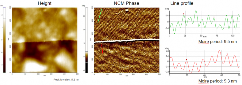
Scanning Conditions
- System : FX40
- Scan Mode: Tapping
- Scan Rate : 3Hz
- Scan Size : 500nm×500nm
- Pixel Size : 512×512
- Cantilever : PPP-FMR (k=2.8N/m, f=75kHz)