-
atomic_steps TyphimuriumBiofilm Reading OpticalWaveguide Morphology FrictionalForce Lattice Mfm sputter CrAu HexagonalBN Annealing temperature_control membrane PVA Defect TPU strontiu_titanate Dimethicone NUSNNI Biofilm Foil Metal Copolymer CrossSection Optoelectronic Hexatriacontane ring shape Bmp Silver KevlarFiber MfmAmplitude Korea 2dMaterials FrequencyModulation
Report image
If you found this image unacceptable, please let us know. We will review your report and take action if we determine this image is really unacceptable.
Semiconductor device, Failure analysis
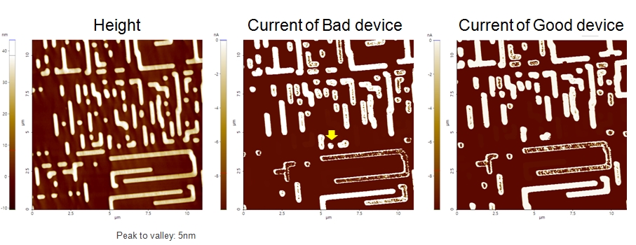
Scanning Conditions
- System: NX10
- Scan Mode: Conductive AFM
- Cantilever: CDT-Contr (k=0.5N/m, f=20kHz)
- Scan Size: 11μm×11μm
- Scan Rate: 1Hz
- Pixel: 512×512
- Sample bias: -0.5V