-
Mfm CuSubstrate Piezoelectric Annealed Layer Optoelectonics OpticalWaveguide SKKU Subhajjit Pinpoint PFM SRAM PolyvinylAcetate Fet PhaseChange InsulatorFilm Scanning_Thermal_Microscopy Filter DNAProtein Indent Mobile MfmAmplitude block_copolymer Anneal LightEmission Pzt PolycrystallineFerroelectricBCZT AtomicSteps DataStorage Hair GaN EPFL Sphere HighAspect Floppy ElectroDeposition
Report image
If you found this image unacceptable, please let us know. We will review your report and take action if we determine this image is really unacceptable.
TSV Cu pad oxidation
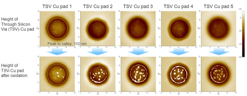
Scanning Conditions
- System : NX-Wafer
- Scan Mode: Non-contact
- Scan Rate : All 1 Hz
- Scan Size : 40μm×40μm
- Pixel Size : All 512×512
- Cantilever : OMCL-AC160TS (k=26N/m, f=300kHz)