New hybrid metrology solutions using advances in automated Atomic Force Microscopy

New hybrid metrology solutions using advances in automated Atomic Force Microscopy
We are delighted to invite you to join our LUNCHEONS on every SEMICON EUROPA day at 12:00 pm, Park Systems Booth B1-357.
Enjoy the lunch snacks and the seminar on: “New hybrid metrology solutions using advances in automated Atomic Force Microscopy,” presented by Haneol Cho, industrial application scientist at Park Systems Europe
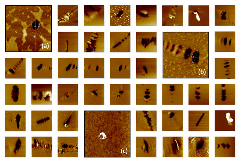
In the 30-minutes presentation, we will be revealing new hybrid nanotechnology techniques that provide a holistic pool of information meeting an even broader range of needs and requirements of semiconductor business like imaging narrow or deep trenches, sidewalls, undercuts, layer thicknesses, defect review, hot spot detection, or imaging material properties locally, and more!
Date: Tuesday, November 16 – Friday, November 19, 2021
Time: 12:00 pm
Place: Neue Messe München, Munich, Germany
The LUNCHEON is open to everyone and is FREE of charge.
Registration and contact: pse@parksystems.com | www.parksystems.com
ABSTRACT
Whether it is just smaller structures or advanced packaging, novel device architecture comes with new challenges for metrology tools to ensure the quality control for failure-free devices. Not only the accuracy of the metrology measurement is of importance but also the throughput, and therefore the overall efficiency in the process.
Despite being generally considered as a time consuming method, Atomic Force Microscopy (AFM) has been widespread and well-established for many years due to its unparalleled precision in imaging real-space 3D features. With recent improvements in the automation of this powerful technique, more and more possibilities arise to tackle the production challenges for high device densities. By directly integrating this versatile technique into other metrology tools, a holistic pool of information can meet an even broader range of needs to control processes involving narrow or deep trenches, sidewalls, undercuts, layer thicknesses, defect review, hot spot detection, or imaging material properties locally. Learn in this talk how the next generation Park Systems AFM can help to increase your efficiency and give you the insights you need to guarantee the best product for your customer.

Image Title
About SEMICON EUROPA
The Semicon Europa is Europe's leading showcase for technologies that are at the cutting edge of the microelectronics industry and highlights the areas of research and development. As an information and communication platform it offers high-caliber technical conferences, forums and programs and excellent networking opportunities. Please visit http://www.semiconeuropa.org/ for more information.
