-
Formamidinium_lead_iodide ChemicalCompound IMT_Bucharest ElectrostaticForceMicroscopy atomic_layer Bio LiquidCell Platinum TransitionMetal IISCBangalore Composite Collagen Dimethicone PolymerBlend Pores TiO2 IIT-chennai Organic Workfunction gallium_nitride Tapping LeakageCurrent Heat LiBattery IRDetector pulsed_laser_deposition Sidewall Heating Hole Indent optoelectronics SmalScan mfm_amplitude EvatecAG Nanostructure
Report image
If you found this image unacceptable, please let us know. We will review your report and take action if we determine this image is really unacceptable.
BN thin film on Si
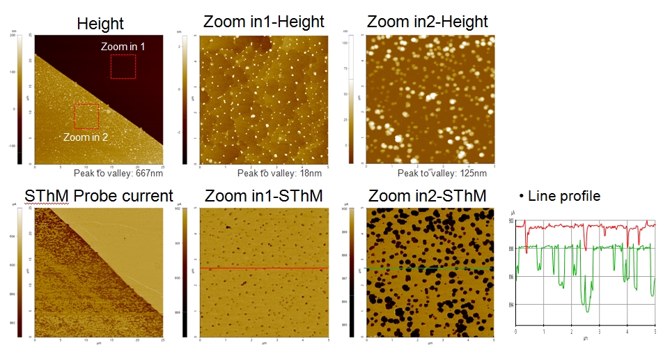
Scanning Conditions
- System: NX10
- Scan Mode:SThM
- Cantilever: Nanothermal probe
- Scan Size: 25μm×25μm, 5μm×5μm
- Scan Rate:0.3Hz, 0.5Hz
- Pixel: 256×256, 256×256
- Scan Mode:SThM
- Cantilever: Nanothermal probe
- Scan Size: 25μm×25μm, 5μm×5μm
- Scan Rate:0.3Hz, 0.5Hz
- Pixel: 256×256, 256×256