-
Cobalt StrontiuTitanate Mfm Pore MagneticForceMicroscopy DOE #EC SAM mechanical_property Nanostructure Temasek_Lab NUS_Physics Inorganic MoS2 OxideLayer WS2 LiquidCell UnivCollegeLondon PrCurve PvdfFilm Steps Mosfet C60H122 Graphite SolarCell Array DLaTGS ThermalDetectors Mapping NeodymiumMagnets Conductive AFM cannabinoid Pores HardDiskMedia membrane
Report image
If you found this image unacceptable, please let us know. We will review your report and take action if we determine this image is really unacceptable.
ITO Film Sputter Deposited onto Silicon
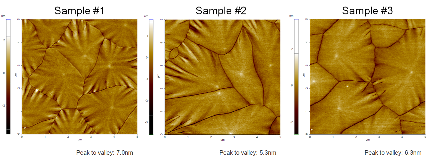
ITO-film, which was sputter deposited onto silicon. The grain size of those samples was influenced by changing the process settings in the Cluterline RAD sputter deposition system, one of the deposition tool platforms manufactured by Evatec.
Scanning Conditions
- System: NX10
- Scan Mode: Non-contact
- Cantilever: PPP-EFM (k=2.8N/m, f=75kHz)
- Scan Size: 5μm×5μm
- Scan Rate: 0.1Hz
- Pixel Size: 256 × 256
- Scan Mode: Non-contact
- Cantilever: PPP-EFM (k=2.8N/m, f=75kHz)
- Scan Size: 5μm×5μm
- Scan Rate: 0.1Hz
- Pixel Size: 256 × 256