-
BaTiO3 self_assembly IISCBangalore light_emitting ContactModeDot Forevision Annealing Yttria_stabilized_Zirconia PpLdpe NUSNNI SSRM HOPG Styrene IcelandSpar LiNbO3 Electrode INSP FAFailureAnlaysis BiFeO3 InLiquid PatternedSapphireSubstrat ferromagnetic Reduction SolarCell IRDetector Molybdenum_disulfide OpticalModulator Tapping Spincast Composition DataStorage conductive Inorganic hydrocarbon H-BN
Report image
If you found this image unacceptable, please let us know. We will review your report and take action if we determine this image is really unacceptable.
Trench Etch Profile on Si Wafer
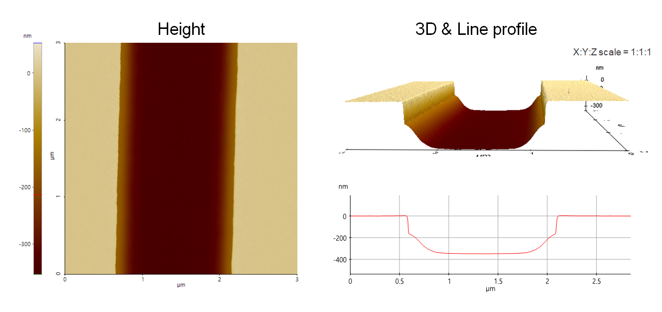
Top dielectric trench etch profile on Si wafer having tapered slope at the trench sidewall.
Scanning Conditions
- System: NX20
- Scan Mode: Non-contact
- Cantilever: AC160TS (k=26N/m, f=300kHz)
- Scan Size: 3μm×3μm
- Scan Rate: 0.21Hz
- Pixel: 1024 × 256
- Scan Mode: Non-contact
- Cantilever: AC160TS (k=26N/m, f=300kHz)
- Scan Size: 3μm×3μm
- Scan Rate: 0.21Hz
- Pixel: 1024 × 256