-
ForceVolumeMapping PUR Barium_titanate Metal OpticalWaveguides Oxidation OxideLayer dielectric trench Oxide Ito Ram Semiconductor Polymer Graphite MagneticArray SiliconOxide Ferroelectric Sperm Sidewall Gallium_Arsenide BCZT GaN OpticalElement Fiber ScanningIon-ConductanceMicroscopy Silicon Epoxy Organic Heat NusEce ForceDistanceSpectroscopy Conducting Annealing Phosphide SolarCell
Report image
If you found this image unacceptable, please let us know. We will review your report and take action if we determine this image is really unacceptable.
PS/LDPE
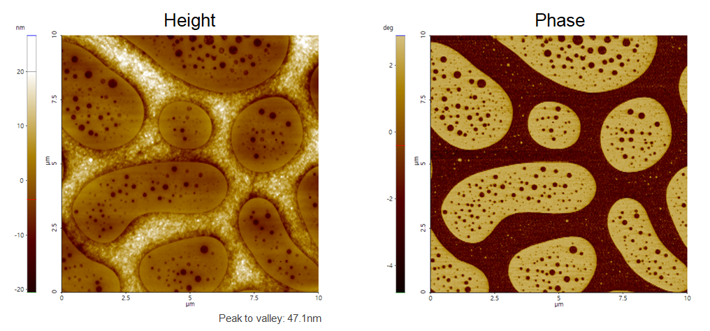
Spincast layer of PS/LDPE blend on Si.
Scanning Conditions
- System: NX20
- Scan Mode: Tapping
- Cantilever: AD40AS (k=40N/m, f=180kHz)
- Scan Size: 10μm×10μm
- Scan Rate: 0.5Hz
- Pixel Size: 512 × 256
- Scan Mode: Tapping
- Cantilever: AD40AS (k=40N/m, f=180kHz)
- Scan Size: 10μm×10μm
- Scan Rate: 0.5Hz
- Pixel Size: 512 × 256