-
ShenYang Granada OpticalElement PolyimideFilm Neodymium ScanningKelvinProbeMicroscopy Polarization Cobalt ContactMode Organic norganic Chungnam_National_University InorganicCompound Dr.JurekSadowski fluoroaalkane Aggregated_molecules NanoLithography PVA Barium_titanate AdhesionEnergy BTO Conduct Tin disulfide Resistance SiliconCrystal Fet MagneticForce FrequencyModulation polyvinyl acetate LateralPFM PatternedSapphireSubstrat Sulfur Crystal STM ito_film
Report image
If you found this image unacceptable, please let us know. We will review your report and take action if we determine this image is really unacceptable.
Photoresist pattern (post-development process)
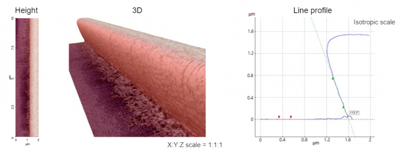
Scanning Conditions
- System : NX-3DM
- Scan Mode: Non-contact
- Scan Rate : 0.1 Hz
- Scan Size : 2μm×10μm
- Pixel Size : 512×2048
- Cantilever : EBD-R2-NCLR (k=45N/m, f=190kHz)